

Abstract
Silicon carbide has recently surged as an alternative material for scalable and integrated quantum photonics, as it is a host for naturally occurring color centers within its bandgap, emitting from the UV to the IR even at telecom wavelength. Some of these color centers have been proved to be characterized by quantum properties associated with their single-photon emission and their coherent spin state control, which make them ideal for quantum technology, such as quantum communication, computation, quantum sensing, metrology and can constitute the elements of future quantum networks. Due to its outstanding electrical, mechanical, and optical properties which extend to optical nonlinear properties, silicon carbide can also supply a more amenable platform for photonics devices with respect to other wide bandgap semiconductors, being already an unsurpassed material for high power microelectronics. In this review, we will summarize the current findings on this material color centers quantum properties such as quantum emission via optical and electrical excitation, optical spin polarization and coherent spin control and manipulation. Their fabrication methods are also summarized, showing the need for on-demand and nanometric control of the color centers fabrication location in the material. Their current applications in single-photon sources, quantum sensing of strain, magnetic and electric fields, spin-photon interface are also described. Finally, the efforts in the integration of these color centers in photonics devices and their fabrication challenges are described.
Export citation and abstract BibTeX RIS

Original content from this work may be used under the terms of the Creative Commons Attribution 3.0 licence. Any further distribution of this work must maintain attribution to the author(s) and the title of the work, journal citation and DOI.
1. Background and introduction
Silicon carbide (SiC) is a complementary metal-oxide-semiconductor (CMOS) compatible material [1, 2] and because of large commercial investments in the last 20 years in the semiconductor industry [3], it has currently a broad range of applications in electronic devices due to the manufacturing of high-quality single crystal wafer. Owing to the perfecting of the material growth in the last decade, SiC has surged as a unique platform for harsh environment power electronics [4]. Due to its broad optical transparency and second-order nonlinear dielectric properties, it has also found some applications since the early 90s in photonics devices, such as waveguides and photonic circuits (photonics crystal and micro-ring resonators) [5] and in optoelectronics [6]. However, the photonics applications have been limited so far due to the lack of commercial availability of SiC on Insulator wafer of adequate quality, currently obtained using the smart cut process [7].
Owing to the improved material quality and purity with less morphological and surface defects and reduction of as grown carbon vacancies (a major limit for electronics), other common defects attributed to deep bandgap point defects (known also as color centers), previously studied in their ensemble formation, could be further studied at the single defect level. By isolating single emitters, quantum light emission can be achieved for applications in quantum cryptography protocols [8]. Additionally, if the quantum state of a single photon can be correlated to the electron spin state of the color centers and the information can be stored in nearby nuclear spins, quantum entanglement between spin and photon can be achieved, permitting, as long term goal, to create a quantum network, which includes quantum communications nodes and quantum memory [9]. As SiC has proved to host these types of color centers, we can now determine that the material has approached the quality needed for quantum applications development.
The first bulk material studied for applications in quantum technology is diamond. It was possible to isolate single color centers and determine their role for application in quantum technologies. As an example, the nitrogen-vacancy (NV) center [10], hosted by the diamond matrix, has become the leading color center in applications such as quantum sensing [11], which is a more achievable application on the road map towards quantum networks. Further, other color centers such as the Germanium vacancy (GeV) [12] and the silicon-vacancy (SiV) [13] in diamond proved to have an enormous potential for quantum optical spin-photon interface due to their narrow bandwidth emission [14]. The wide bandgap of the diamond, together with its weak spin–orbit coupling and diluted nuclear-spin bath, gives to diamond color centers a remarkable spin coherence, and isotope engineering can enhance it further, due to the possibility of growing highly pure samples [15]. SiC also enjoys most of these properties, and benefits from mature production protocols on a large scale which are available for silicon, excellent nanofabrication quality [16], and capability of ion implantation without the side effects typical of the diamond, such as graphitization during irradiation [17]. However, diamond has some limitations in this respect in terms of scalability, electrical control, integration and fabrication and other material platforms are sought after to further advance this field of applications. Some of the SiC intrinsic and extrinsic point defects hold competitive properties that, if integrated with the material scalability and control, could advance the current state of the art.
SiC offers an alternative platform for integration of quantum systems in large scale wafers as well as suitability for nanofabrication and great potentials for integrated quantum photonics [2], owing to its second-order nonlinearity, low two-photon absorption, and optical transparency. However, challenges are still in both the material fabrications for integrated photonics and the color centers' generation and control [18]. An even more exciting field for quantum devices in SiC [19] can be found in its electrical excellent properties and electrical device fabrication, that is by far more established than photonics, as SiC is used in high power electronics [20] and in metal-oxide-semiconductor field-effect transistor (MOSFET) [21]. Electrically controlled quantum devices can be envisioned for the detection of spin signals and single-photon excitation [22–25], however, integration of electrically and optically controlled devices appear at an early stage.
SiC and other materials have been proposed as a platform for spin-based photonic quantum technologies. The light–matter interface relating quantum light states and the quantum emitter internal states (electron spin) can be used to constitute quantum circuits and networks [26], where quantum entanglement distribution and storage is performed [27]. Solid-state emitters can perform such interfacing role in a scalable and in a compact way due to their atom- and ion-like properties. The practical implementation of future quantum network nodes (figure 1(A)) needs the fabrication and control of many spin-photon interconnects (figure 1(B)), integrating many quantum emitters within photonic circuits in a compact and efficient manner. This scaling challenge is driving engineering efforts to go beyond the current state of the art, which is of only 'two' spin-photon quantum systems [9]. This has recently stimulated the investigation of scalable and amenable to integration solid-state quantum emitters materials. These circuits are central to implement scalable spin-photon interconnects for the development of quantum networks for entanglement distribution between distant quantum nodes (figures 1(A) and (B)). One promising approach is to connect stationary qubit (spin qubits) nodes using photons and in some of these nodes, a quantum memory (based on nuclear spins) makes use of ancillary qubits to establish single-qubit and two-qubit operations. If one qubit in a node strongly couples via an optical channel communicating with other nodes, these nodes can be entangled with high fidelity using heralded optical measurements. Currently spin-photon interconnects are at the core of novel nanophotonic, nanoelectronics and spintronics architectures, used to transfer the information of electrons' spin to photons within an optical circuit. An immediate application of spin-photon interconnects is the establishment of integrated and on-chip novel sensing and imaging platforms at the micro and nanoscale, while a long-term application relies on the development of a quantum networks.

Figure 1. (A) Representation of a quantum network where users can communicate quantum operations results via quantum communication channels using photons and quantum repeaters (in yellow). (B) Entanglement distribution between quantum memories (bound nuclear spins) using spin-photon interconnects formed by a color center with quantum emission of single-photon and optical/electrical control of its spin quantum state. (C) Summary of quantum emitters in different solid-state platforms for the spin-photon interface. (D) The main future goal for integrated quantum photonics spin-photon node: planar spin-photon interconnects within monolithic quantum photonic integrated circuits in 4H-SiC on Insulator platform.
Download figure:
Standard image High-resolution imageRecent reviews have identified some prominent and emerging semiconductor materials for spin-photon interconnects, including spin defects in diamond, SiC, rare-earth ions in solids, and novel 2D quantum materials [26, 28]. Here, the projected evaluation is focused only on criteria that encompass the availability of single-photon emission, long electron spin coherence time and electron spin coupling with nearby nuclear spins in a scalable platform. It is to be mentioned however that established platforms such as quantum dots and atom-cavity systems have clearly demonstrated that they possess excellent spin photon interconnects characteristics [29, 30]. These platforms may have short electron spin coherence time, not clear nuclear spin ancilla qubit or scalability issues. Among the above-mentioned platforms, while diamond is leading the scene in terms of proof of feasibility and availability of single-photon emitters, it is understood it may not be sufficiently scalable for multiple emitters integration and it lacks telecom wavelength quantum emission, while SiC and novel 2D materials could provide a better platform for quantum emitters integration. Between SiC and novel 2D materials, SiC can host single-photon sources and spin qubits in the same color centers [28] with a wide variety of emission wavelengths up to the infrared, while the latter so far have shown only single-photon emission, while optical spin control is not yet fully understood, neither ancillary qubits have been identified. A comparison of the spin-photon interface in various solid-state platforms is shown in figure 1(C), where the above criteria for the quantum emitters are shown such us, emission region of zero phonon lines (ZPLs), spin coherence time and available ancilla qubits. For more details on the comparative properties of these and other platforms, the reader should refer to [26, 28].
Spin and optical stability at the single defect level and related reliable manufacturing are requirements for quantum technology to be implemented, making SiC one of the foremost light–matter quantum interfaces available, competing with diamond and atomically thin semiconductors for this role. Especially single-photon emitters in SiC are now attracting attention for quantum photonic applications [28] and their proven spin-photon interface capability, however, the integration in planar photonic circuits as in figure 1(D) remains a challenge. SiC is available in nature in more than 200 polytypes, and all of them show bandgaps around 2–3 eV [31], much larger than Si. This makes SiC a suitable candidate for high-temperature electronics [32]. It is also promising in high-power electronics since it has breakdown voltage 10 times larger and thermal conductivity 3 times larger than Si [31, 32], as well as in the microelectromechanical system (MEMS) applications [33]. Sensor applications receive help from the positive electrical properties of SiC, as well as the availability of mature doping technologies, for fields such as optical sensors for UV and x-ray, and gas sensors [34]. Biotechnology applications are favored by the biocompatibility and the chemical inertia of SiC [35].
In this paper, we will review recent advances in SiC color center studies, fabrication and quantum control, with the focus to the last five years of efforts after the first surge of interest [36]. We first focus on categorizing the color centers with respect to their quantum properties, showing their key studies to assess their quantum properties, benchmarked to the performance criteria needed for the applications, highlighting the major achievements that could allow in terms of integration and fabrication to move towards the implementation of scalable spin-photon entanglement. Specifically, we focus on point defects (primarily vacancies related) in SiC, which have been considered as potential physical systems to realize quantum devices such as single-photon sources and spin-photon interface for quantum interconnects as described in figures 1(B) and (D). Other applications in quantum sensing that rely in quantum coherent manipulation of the color center spin states are also described. It is to be noted that quantum sensing applications are much less demanding of spin-photon quantum networks.
SiC color centers or point defects act as isolated quantum systems for quantum sources and optical and electrical spin control. As the short immediate term goal has been to identify these systems in the material, as the medium-term goal, the same optical and spin interface can be used for electric and magnetic field sensing. The color centers are brought to an excited state via pumping by a laser or an electrical current. One photon is then emitted during the decay from excited to the ground state. In some of these defects with the high spin state, the decay into the intersystem crossing allows modulation of their photoluminescence, via also further excitation of the ground state using a microwave or radiofrequency pump. This permits to prepare and measure their spin state polarization. This property can be used for quantum sensing applications or to establish a spin-photon interface. By interacting with other sources of static and variable magnetic fields at a nanometric distance from the emitters, their spin transition frequency is shifted and their coherence time is reduced. This effect is used to establish quantum sensing.
The best-known point defect in SiC is the divacancy (DV), which closely resembles the NV center in diamond, albeit with slightly different performances. Compared to NV centers in diamond, the DV in SiC may have slightly worse quantum properties, but it certainly has better manufacturability. The role of paramagnetic defects in SiC to achieve optical and spin quantum coherence control is discussed in [37]. The promising future for quantum applications is highlighted in [38, 39].
2. Quantum properties of silicon carbide color centers (ab initio and experiment)
SiC can host many color centers with quantum properties as reviewed in a previously mentioned work [26], many of which are active upon interaction with an optical pumping with energy below the bandgap energy, and are typically originated mostly by vacancies of either carbon or Si, in addition to substitutional impurities, such as transition metal (TM) impurities (Ti, Cr, V, Mo, Er, etc) and other impurities such as most common N. In figure 2 a summary of the emitters in SiC found to have quantum properties such as single-photon emission and or optical spin polarization are shown versus their photoluminescence range, ZPL and their spin properties (zero field splitting (ZFS)).

Figure 2. Color centers in SiC plotted versus their observed ZPL by PL measurements and their spin ZFS from electron paramagnetic resonance (EPR) or optically detected magnetic resonance (ODMR) measurements (left) for spin defects with proved optical spin polarization. Among these the VSi [40] VCVSi, [41, 42] the NCVSi [43, 44] in various polytypes. In addition, some transition metal color centers such as Ti [45], V [45–47], and Mo [48]. On the right in red, color centers in SiC observed as single-photon sources with the maximum brightness observed in cts s−1, among this the CAV [49, 50], SiC [22], oxidation [22] and annealing [51] related and unknown, 3C IR emitters [52].
Download figure:
Standard image High-resolution imageSuperscripts with parentheses on the defect names show the charge states. The most popular defects are those labeled VSi(−) (V1, V2, V3) and VSiVC(0) (PL1–PL4, QL1-6, ky5), where VSi stands for silicon vacancy and VSiVC is a divacancy of C and Si. The most studied defects are the neutral divacancy or VSiVC(0) and negatively charged Si vacancy (VSi) in the 4H-SiC and 6H-SiC polytypes [53–64]. While most of the defects were found more than 10 years ago with ensemble PL and EPR studies, however, the current studies aim to determine more accurately their quantum properties due to newly established methods of single-photon detection, single-color center isolation and quantum coherent spin control. These methods allow to review some of the past identification with more accurate approaches and associate more precise modeling based on ab initio calculations, thus not only advancing the quantum technology field of interest but also adding further fundamental knowledge of these defects in SiC. In addition to photoluminescence (PL), in fact, other parameters are used to describe the quantum properties of the color centers. The zero-phonon line (ZPL) and the phonon sideband together make the line shape of individual light-absorbing and emitting molecules [65]. The Debye-Waller factor (DWF) describes the thermal motion attenuation of x-ray or coherent neutron scattering [66]. DWF can be estimated with the ratio of the ZPL PL emission, compared to the total PL emission, which is the combination of the ZPL PL emission and the phonon-broadened PL. The ZFS refers to the 'lifting' of degeneracy in the absence of a magnetic field unpaired electrons interact to give two or more energy states [67]. Finally, ODMR is a technique to optically pump the electron spin state of a crystal defect for spin initialization and readout [68]. The main goal of these studies is to assess these color centers in terms of quantum properties, as such here we only review the emitters that present interesting potentials as a qubit or as a single-photon source or in quantum nanophotonic.
The defect labeled VSi(−) known also as TV1–TV3 as reviewed in [26] is studied in [54, 56, 58, 60, 62, 69–77]. The spin number is 3/2 (it was previously assigned to an S = 1 [54]). The ZPLs are 862 nm (V1), 858.2 nm (V1') and 917 nm (V2) for polytype 4H; and 865 nm (V1), 887 nm (V2) and 907 nm (V3) for polytype 6H. The V1,2,3 corresponds to the 2 or 3 inequivalent sites of the VSi(−) in 4H and 6H polytype. V1 and V1' are the hexagonal site locations corresponding to two different excited states (V1' corresponds to the higher energy excited state). This emitter has been found in polytypes 4H, 6H, and 15R, while it is not found in 3C. Both V2 and V1 lines in the 4H polytype has been proven for optical coherent spin control. In particular, the V2 line has been mostly studied as qubit with ZFS of 70 MHz, the V2 maximum ODMR signal (∣ΔPL/PL∣) by off-resonant optical excitation is 1.8% when the V2 center is embedded in nanopillars [18] (0.4% when in bulk material). The largest PL intensity for V2 is 10 kcps s−1 without a solid immersion lens using a Si detector with 20%–30% quantum efficiency [78] and 40 kcps with a solid immersion lens [69]. It was shown that this center features polarization-selective transitions to two spin ground states [79], where some of the hexagonal polytypes show ZFS stable over a large temperature range from 10 to 320 K [147], remarkable for use in sensors. It is possible to use them also for stimulated microwave emission as they support optically induced polarization inversion [59]. This center presents ODMR for both the V1 and V2 line in 4H SiC up to the single defect level, as well as single defect coherent spin control with coherence time up to 0.6 ms [73]. V1' line ODMR has not been observed. Due to weak PL for the V2 emission, solid immersion lens (SIL) or nanopillars are used to achieve spin optical control and ODMR with single color centers at room temperature, otherwise optical spin control can be achieved by exciting with the laser direction orthogonal to the c axis for ensemble emission [80], as this color center dipole is primarily along the c-axis.
The V1 and V1' were recently studied as a qubit, the first proving to be a better option for spin-photon interface than V2 [73, 76], which is much dimmer and not always can be generated and observed. The V1 in 4H DWF is 40% [73]. The V1 ZFS is 4 MHz in the ground state. The maximum ODMR signal (∣ΔPL/PL∣) by on-resonant optical excitation is 100% and it is observed as a positive signal at 170 MHz using a B = 60 G and at low temperature. By off-resonance excitation, the V1 line has an extremely low negative ODMR contrast. The V1' line is polarized with the laser field perpendicular to the c axis and V1 with the laser field parallel to the c axis (as V2). As most SiC wafers are grown few degrees off the c-axis [80], laser excitation from the edge of the sample will increase the polarization of V1 and V2, while excitation directly on the face of the chip will provide mostly emission of the V1' (figure 4(A)). The V1 line spin control can be achieved only at low temperatures and by in resonance excitation. Due to millisecond-long spin coherence times originating from the high-purity crystal, high-fidelity optical initialization of the spin state and its coherent spin control can be achieved. Further, it was achieved coherent coupling of the electron spins to single nuclear spins with ∼1 kHz resolution [76]. This center is currently the most promising for quantum network implementation in isotopically purified 4H SiC.
Only recently the VSi(−) role as qubit and charge state have been fully identified by means of high-precision first-principles calculations and high-resolution EPR resonance measurements, as an isolated negatively charged silicon-vacancy and it is associated to so-called V1 line being a V(−)Si at h (hexagonal)-site and V2 a V(−)Si at k (cubic) site for 4H-SiC [40], as for 6H V(−)Si the V1 is an h-site, V2 is a k2 site and V3 a k1 site [42]. In figures 3(A)–(C) the comparison between the cubic 3C and hexagonal 4H and 6H polytype SiC stacking layers seen from the top along the main crystallographic axis c, where the atoms of Si and C are shown along axis c or off-axis in different cubic h sites or hexagonal sites-k. For a single vacancy, it is expected that it occupies one of the 2 sites in 4H and 3 sites in 6H, as such the ZPLs are 2 or 3, plus excited state doublet. V2' has never been observed.

Figure 3. Defects locations in SiC: (A)–(C) Primitive cells for 3C, 4H, and 6H-polytype. Brown upper-case letters show the stacking of Si–C double layers, while lower-case letters show whether the double layers and their immediate surroundings follow a cubic like (k) or in a hexagonal-like (h) stacking order. Green lower-case letter pairs show variants of a pair defect [41]. V1−V2 silicon-vacancy related qubits in 4H-SiC. (D) Nonequivalent atomic sites in the primitive cell of 4H-SiC. (E) Isolated vacancy model and the assignment of V1−V2 centers to the different silicon-vacancy configurations in 4H-SiC [40]. Images (A), (B), and (C) reproduced from [41] Davidsson, Ivády, Armiento, Son, Gali and Abrikosov 2018 First-principles predictions of magneto-optical data for semiconductor point defect identification: the case of divacancy defects in 4H-SiC New J. Phys. 20 023035. 10.1088/1367-2630/aaa752. Paper published under the terms of the Creative Commons Attribution 3.0 license. Images (D) and (E) Reprinted with permission from [Ivády, Davidsson, Son, Ohshima, Abrikosov and Gali 2017 Identification of Si-vacancy related room-temperature qubits in 4H silicon carbide Phys. Rev. B 96 161114] 10.1103/PhysRevB.96.161114. Copyright (2017) by the American Physical Society.
Download figure:
Standard image High-resolution imageThe defect labeled DV(0) [81] (figure 4(C)) quantum properties were studied in 4H-SiC and associated to the PL1–PL4 lines in [53, 55, 82–86]. It is currently associated with an S = 1 VSiVC(0), with ZPLs corresponding to the 4 non-equivalent sites, as following, PL1 occupying the hh site, PL2 kk site, PL3 kh, and PL4 hk site [41, 42]. ZPLs are in the range 1078–1132 nm with ZFS of 1.224–1.336 GHz in the ground state and 0.75–0.95 GHz in excited states. Other emissions named PL5 and PL6 have comparable properties but are not fully identified. As a single color center, the largest PL intensity is 27 kcps s−1 with a millisecond spin coherence time [83]. This is the maximum value at low temperature using a superconducting nanowire detector with 80% quantum efficiency. The DWF for the center is 5%. The maximum ODMR signal by off-resonant optical excitation is 5%–6% [85]. The defect labeled with ZPLs QL1–QL6 = 1093–1140 nm is a VSiVC(0) in 6H polytype [82]. ZFS is 1.3–1.38 GHz in ground states. The maximum ODMR signal by off-resonant optical excitation is <0.001. Its full identification has been recently proposed [42].

Figure 4. The VSi, CAV(+), DV(0) lines and NV in SiC are spectrally shown below. (A) VSi in a hexagonal 4H SiC crystal emission at 70 K, where the ZPLs(V1 V1' and V2) of the 2 inequivalent sites are shown [49]. Here the sample is excited from the edge to enhance the emission of V1 and V2 lines, V1' results less bright. (B) PL emission of the CAV(+) at 70 K. Images (A) and (B) reprinted by permission from [Springer Nature Customer Service Centre GmbH]: [Springer Nature] [Nature Materials] [A silicon carbide room-temperature single-photon source, Castelletto, Johnson, Ivády, Stavrias, Umeda, Gali, and Ohshima), [COPYRIGHT] (2013). (C) Lay-out of the DV(0) in the two axial and basal locations in 4H SiC [99], with their PL1–4 as measured at 20 K [53]. Comparison with the ab initio simulations assigning the site location to each PL lines compared with the predicted values [41]. Image (C) on the left reproduced from [86] Castelletto, Rosa and Johnson (2015). Silicon Carbide for Novel Quantum Technology Devices, Advanced Silicon Carbide Devices and Processing, Saddow and La Via, IntechOpen. This chapter is distributed under the terms of the Creative Commons Attribution 3.0 License. Image (C) on the top right reprinted by permission from [Springer Nature Customer Service Centre GmbH]: [Springer Nature] [Nature] [Room temperature coherent control of defect spin qubits in silicon carbide, Koehl, Buckley, Heremans, Calusine and Awschalom), [copyright] (2011). Image (C) on the bottom right reproduced from [41] Davidsson, Ivády, Armiento, Son, Gali and Abrikosov 2018 First principles predictions of magneto-optical data for semiconductor point defect identification: the case of divacancy defects in 4H-SiC New J. Phys. 20 023035 10.1088/1367-2630/aaa752. Article licensed under the Creative Commons Attribution 3.0 license. (D) Lay-out of the NCVSi in the two axial and basal locations in 4H-SiC with its spectral emissions [44]. Images (D) reprinted with permission from [Zargaleh, Eble, Hameau, Cantin, Legrand, Bernard, Margaillan, Lauret, Roch, von Bardeleben, Rauls, Gerstmann and Treussart 2016 Evidence for near-infrared photoluminescence of nitrogen vacancy centers in 4H SiC Phys. Rev. B 94 060102] Copyright (2016) by the American Physical Society.
Download figure:
Standard image High-resolution imageThe defect labeled Ky5 is the divacancy in polytype 3C at 1127 nm is studied in [82, 85]. The largest PL intensity at the single level is 26 kcps. DWF is 7%. ZFS is 1.3 GHz in ground states. The maximum ODMR signal by off-resonant optical excitation is 0.075. This defect has been studied as a high fidelity spin-photon interface platform for the quantum network [85].
A single-photon source based on an emitter ranging from 1085 ÷ 1225 nm in 3C polytype has been discovered using superconducting single-photon detectors with a single-photon emission at 900 kcps s−1, which is a record brightness at room temperature at this wavelength [52]. Due to the large variability of the emission the color center could not be associated with Ky5, as well DV can be observed as SPS only at low temperature and they are very weak (27 kcts s−1 at saturation). These emitters may be related to stacking faults usually present in hetero-epitaxial 3C-SiC layers. The PL is the result of the exciton recombination process of electrons and holes. The hole is tightly localized at the point defect while the electron's position is loosely localized due to the stacking faults. Similarly, a high brightness emitter at 1400 nm was recently investigated in a commercial 4 μm membrane of 3 C SiC. SPS in the emission region are excited at 975 nm and detected using single-photon superconducting nanowires detectors with 90% quantum efficiency.
The defect labeled CAV, where CAV stands for carbon anti-site-vacancy pair, found in polytypes 4H, 6H, and 3C is studied in [49, 87, 88]. The CAV pair is a fundamental defect in SiC. It is a counterpart of the VSi and can be created by high-energy-particle radiation and subsequent annealing at 700°–750°. One of the four configurations of this defect CAV(−) state has been identified by EPR in n-type 4H-SiC [89]. The positively charged state of the CAV(+) defect has also been identified in 4H-SiC [90]. The CAV(+) was the first single-color center to be isolated in SiC, carrying a positive charge and offering a bright room-temperature photon emission at ∼700 nm wavelength [49]. Eight ZPLs were identified due to 4 inequivalent sites with 2 excited states and are also known as AB-lines (figure 4(B)), such as A1 = 648.7 nm (higher energy excited state of A2), A2(hh) = 651.8 nm, A3 = 665.1 nm (higher energy excited state of A4), A4(hk) = 668.5 nm, B1 = 671.7 nm, B2(kk) = 673 nm, B3 = 675.2 nm, B4(kh) = 676.5 nm. The largest PL intensity measured as single emission is 2000 kcps s−1, and the spin number is ½. No ODMR has been observed from this defect. This emission has been associated with isolated single-photon sources. CAV was also studied in 3C SiC as a possible single-photon emitter [88].
Previous identifications were associating this emission with its neutral charge state [91], which has, however, emission in the infrared based on ab initio simulations [87]. The ground state spin of the neutral pair is S = 1 and is predicted useful for coherent manipulation and optical addressing, much like the NV-center in diamond, with a better emission in the infrared at telecom wavelength. It is also shown from previous studies, that CAV(0) is not accessible in n-type and p-type materials and it has been studied recently in ultrapure isotope-enriched 4H-28SiC [92]. In such pure and compensated materials, the CAV(+) was easily activated by low energy photons above 1.1 μm, and photons with energies below 1.1 μm can excite electrons from the CAV(0) level to the conduction band, thus transforming CAV(0) to CAV(+). The CAV(+) was detected by EPR. Finally, with photons of higher energy and wavelength shorter than 539 nm, the light can also excite electrons from the valence band to the CAV(+) level and change their charge state from positive to neutral. By careful design of the material purity, the CAV(0) can be controlled by optical excitation and converted from CAV(+).
The defect labeled SiC (D1) in [26], of polytype 4H, is studied in [22]. It has ZPL 540–689 nm, with the largest PL intensity >300 kcts s−1 when electrically driven and 900 kcts s−1 when optically driven. The spin number is ½. The D1 center (SiC) is stable to high temperature has a high C3v symmetry with polarization perpendicular to the c axis and ZPL at 427 nm. The luminescence mechanism can be described as the recombination of the electron at the split conduction band state and a localized hole on the defect site. Due to the large variability of the ZPLs observed of 200 nm, the model predicts the defect to reside close to the stacking fault (SF), as the ZPL energy follows the variation in the conduction band edge induced by the SF. The position of the defect at a nanometric distance from SFs may explain such variability of ZPLs. However, further studies have found that similar emission can be achieved by the oxidation process in all polytypes 3C, 4H and 6H and by annealing. The defect labeled 'Oxidation related' in [26] of polytype 3C, 4H and 6H, is studied in [93]. It has ZPL 564–690 nm, with the largest PL intensity 800 kcts s−1. The defect labeled 'Annealing related' in [26], of polytype 4H, is studied in [51]. It has ZPL 564–620 nm, largest PL intensity 2000 kcps s−1, DWF 33%.
The defect labeled NCVSi(−) (NV) (figure 4(D)) in SiC has gained consideration after its prediction and eventual experimental verification after preliminary PL and EPR studies, confirming its formation in an n-type substrate. NCVSi (NV) is studied in [43, 44, 94, 95]. NV stands for nitrogen-vacancy pair with spin number 1. ZPLs are associated with PLX1-4 in 4H corresponding to kk, hh, hk and kh, from 1180 to 1242 nm, with ZFS from 1.183 to 1.328 GHz. In 6H SiC only 3 ZPLs associated with the axial sites h, k1 and k2 were measured at 1291, 1305 and 1240 nm with ZFS of 1.3–1.4 GHz. In polytypes 3C the ZPL is at 1468 nm and ZFS at 1.3 GHz [43, 44]. Its optical spin polarization of the ground state has been just recently demonstrated [96] with ODMR signals of NV centers (hh, kh) in 4H-SiC at 1316.5 MHz and 1328.6 MHz, observed at room temperature, as well single-photon emission of this color centers has been demonstrated at room temperature in a 30 keV nitrogen implanted 4H-SiC with emission range from 1150 to 1350 nm and lifetime of 2 ns [96]. The coherence time from Ramsey interference is 1μs in an ensemble of emitters.
Emission in the telecommunications bands can be achieved by doping with TM impurities [41–43, 97, 98], allowing in some cases for ODMR [41, 43].
Now we will discuss some TM color centers. The TM atom sits on a pure substitutional Si site (TMSi) or can occupy a divacancy site TMSiVC. The defect labeled Ti(0) in is the neutral charge state of Ti titanium impurity, found in polytype 4H, 6H, 12R and 15R, and studied in [100]. It has ZPLs from 433 to 450 nm, spin number 1, ZFS between 10–11 GHz and maximum ODMR signal >0.05. These color center quantum properties are currently not very well-known and are still a yet to be understood system. Apart from Ti, several TM impurities in SiC do emit at and near telecom wavelengths, but knowledge about their spin and optical properties is yet incomplete. The most studied are Cr, V, and Mo in SiC. Additionally, the ZFS tends to be at high frequency as such a combination of optical coherent spin control in presence of magnetic field combined with traditional ODMR can be used to determine the inhomogeneous spin transitions broadening of these defects.
The defect labeled Cr3+, where Cr stands for chromium impurity, of polytype 6H, is studied in [45]. It has spin number 3/2 and ZFS >40 GHz. The defect labeled Cr2+ of polytype 6H is studied in [45]. It has ZPL 1033–1127 nm, the spin number is 2 and ZFS is 39 GHz. The defect labeled Cr4+ in [26], of polytype 4H and 6H, is studied in [45, 101, 102]. It has ZPL 1142–1181 nm, DWF 75% from ensemble measurement, the spin number is 1, ZFS 1–6.7 GHz, maximum ODMR signal by on-resonant optical excitation 100%. Cr4+ defect ensembles created by ion implantation of 4H-SiC have shown spectral-hole linewidths much narrower than as-grown defects, and the possibility of exciting them by near-IR light. The defect has a cryogenic T1 of the spin-1 electronic ground state longer than the optical transition relaxation time, a high ZPL emission of 73%, and a narrow linewidth of the inhomogeneous optical ensemble of <7 GHz [45]. It was measured optically and using ODMR a ZFS of 6.1 GHz. The inhomogeneous spin coherence time is 37 ns. These features make this color center interesting for quantum information in solid-state, however, due to the long lifetime of Cr in SiC of 145 μs this emission cannot be used for the spin-photon interface, but it could be used for optical quantum memory.
Vanadium (V) is one of the oldest known defects in SiC, as it was routinely used for compensation of impure crystals. First optical studies showed strong and sharp luminescence lines, as well as narrow EPR features [46]. The defect was further found to have multiple charge states, which are of interest for spin-to charge conversion [47]. The negative charge state V(−) (also known as is V3+) in for polytypes 4H and 6H, is studied in [45]. It has ZPL 2000 nm, spin number 1, and ZFS 0.7–11 GHz. The defect labeled V(0)neutral charge state (also known as V4+) in [26] of polytypes 3C, 4H, 6H, and 15R is studied in [45]. It has ZPL 1300–1550 nm and spin number ½ [46]. In the neutral charge state, vanadium defects in 4H SiC have been studied by group theory and ab initio DFT supercell calculations, predicting emission at wavelengths of a doublet at approximately 1.28 μm and a single line at 1.33 μm, known as α and β lines. The doublet has been attributed to the hexagonal site, the single line to the quasi-cubic site and they are showing optical lifetimes of 163 ns and 43 ns, respectively [47]. These emissions can be of interest for quantum photonics due to the spectral region ideal for cavity enhancement and the short lifetime, as such single-photon emission could be verified, however, it is not clear if their spectral purity can be used as a spin-photon interface. Resonant spectroscopy will be needed to shed further light on the nature of their decay processes, including nonradiative decay channels and thermally enhanced decay rates. The optical properties of this charge state have been recently studied in [103] by implanting near-surface isolated single vanadium dopants in 4H and 6H-SiC emitting in the region 1278–1388 nm, and with brightness allowing cavity-free detection. Optically detected magnetic resonance in the ground and excited, and coherent quantum control of the spin-orbital states is demonstrated. Single-photon emission is also demonstrated at low temperatures and with in-resonance excitation. This work shows that V impurities in SiC have hyperfine interactions with the vanadium nuclear spin and clock transitions for quantum memories, as well can be used as quantum telecom emitters.
The defect labeled Mo(0) where Mo stands for molybdenum impurity, of polytypes 4H, 6H, and 15R is studied in [45]. It has ZPL at 1033 nm, spin number 1, and ZFS 3.3 GHz. In [48] a Mo impurity with ZPL transitions at 1076 nm (in p-type 4H-SiC) and 1121 nm (in p-type 6H-SiC) were studied. These impurities were associated with the Mo5+ (4d1) charge state with S = 1/2 for both the electronic ground and excited state. An all-optical identification and coherent control of Mo-impurity spins in the presence of a small magnetic field were achieved which show an optical lifetime of ∼60 ns and an inhomogeneous spin dephasing time of ∼0.3 μs, establishing this defect as a relevant alternative for quantum spin-photon interfacing. Due to the short optical lifetime and the acceptable spin coherence time this emission can supply an alternative platform for spin-photon entanglement distribution.
Er3+ in SiC has also been studied for emission at 1540 nm which offers promising potential for the development of semiconductor light-emitting devices at a wavelength within the fiber-optics transparency window [104]. As per the quantum communication engineered photonics cavity with Er in SiC could be used for quantum memory.
In figure 5(a) summary of most relevant defects, with PL, spin properties and the determination of the ground state spin polarization, among these defects CAV, VSi, DV, NV, and V were isolated at the single level.

Figure 5. Summary of the SiC color centers where single-photon emission (*) and single spin coherent control have been demonstrated (↑, dashed where spin state and polarization are known to exist, but spin control has not been achieved yet).
Download figure:
Standard image High-resolution imageIn table 1 the details of the most relevant characteristics of the above-described color centers based on the above references, are presented.
Table 1. Summary of the color centers with ZPL, spin, ZFS, DWF, saturation count rate, lifetime, spin coherence time. Data for VSi are from [54, 56, 58, 60, 62, 69–73, 76–79, 147]; DV from [53, 55, 81–85]; IR unknown emitters from [52]; CAV form [49, 87–90, 92]; D1 color centre from [22] and related references.; oxydation related defects from [93]; annealing related from [51]; NCVSi from [43, 44, 94–96]; Ti from [100]; Cr from [45, 101, 102]; V from [45–47, 103]; Mo from [45, 48].
| Color centres | ZPLs (nm) | Spin | ZFS (GHz) | DWF (%) | Single photon saturation counts rate (kcts s−1) | Optical transition lifetime (ns) | Electron spin coherence time (ms) |
|---|---|---|---|---|---|---|---|
| VSi (4H-SiC) | 0.862 (V1), 0. 858 (V1'), 0. 917(V2) | 3/2 | 0.070 (V2), 0.004(V1) | 40 (V1) | 8–10 (V2), 12 (V1), 4 (V1') | 6.2 (V2), 5.5 (V1), 5.6 (V1') | 0.6 (V1), 20 (V2) |
| VSi (6H-SiC) | 0.865 (V1), 0.887 (V2), 0.907 (V3) | 3/2 | 0.00278 (V1), 0.128 (V2), 0.266 (V3) | ||||
| DV (4H-SiC) | 1.078, 1.108, 1.131, 1.132 | 1 | 1.334, 1.224, 1.305, 1.336 | 5 | 27 | 14 | 1 |
| DV (6H-SiC) | 1.093, 1.108, 1.124, 1.135, 1.140 | 1 | 1.347, 1.383, 1.236, 1.334, 1.300 | ||||
| DV (3C-SiC) | 1.127 | 1 | 1.300 | 7 | 26 | 18.7 | 0.9 |
| 3 C unknown | 1085–1225 | unknown | 900 | 0.81 | |||
| CAV(+) (4H-SiC) | 0.6487, 0.6518, 0.6651, 0.6685, 0.6717, 0.673, 0.6752, 0.6765 | 1/2 | 2000 | 1.8 | |||
| D1 (4H-SiC) | 0.540–0.689 | 1/2 | 900 | 2–5 | |||
| Oxidation | 0.564–0.69 | 800 | 1–3 | ||||
| annealing related | 0.564–0.62 | 33 | 2000 | 2.0–2.2 | |||
| NCVSi (4H-SiC) | 1.180, 1.223, 1.241, 1.242 | 1 | 1.193, 1.282, 1.328, 1.331 | 17.4 | 2.7 | 0.001 (T2*) | |
| NCVSi (6H-SiC) | 1.328, 1.278, 1.345 | 1 | 1.291, 1.305, 1.240 | ||||
| NCVSi (3C-SiC) | 1.468 | 1 | 1.303 | ||||
| Ti | 0.433, 0.435, 0.44, 0.45 | 1 | 10–11 | ||||
| Cr2+ | 1.033–1.127 | 2 | 39 | ||||
| Cr3+ | Unknown | 3/2 | >40 | ||||
| Cr4+ | 1.142–1.181 | 1 | 1–6.7 | 75 | 135 000 | 0.000 0370 | |
| V3+ | 2 | 1 | 7–11 | ||||
| V4+ (SiC-4H) | 1.279, 1.335 | 1/2 | 529–43 | <25,<50 | 167,45 | 0.0002–0.0012 | |
| V4+ (SiC-6H) | 1.309, 1352, 1389 | 1/2 | 524, 25, 16 | <45,<40,<40 | 108,11,31 | ||
| Mo (SiC-4H) | 1.076, 1.121 | 1/2 | 3.3 | 60 | 0.0003(T2*) |
Due to the large variety of color centers available in this material, it is challenging to determine the best use of them for quantum technologies as it would depend on the specific application. The visible emitters appear promising as single-photon sources, however, their uncontrollable formation poses a limit for further development in useful technology. While emission in the IR is more promising for single-photon source, so far it suffers either from their unknown defect origin, low brightness and need of the low-temperature operation. The quantum spin control properties for applications in the future quantum network appear more promising for emitters such as VSi or VSiVC (DV) as in this case low temperature and resonance excitation is needed to achieve entanglement distribution. Finally, the 'optimal' emitter which should combine IR emission, quantum spin manipulation at room temperature, ancilla qubits, and localization fabrication control, may still to be found, possibly the NCVSi seems to provide all these characteristics, albeit the ODMR contrast it is quite low with off-resonance excitation. Further study will demonstrate the potentials of these centers.
3. Defects fabrication: material growth and irradiation
The material doping influences the formation of the color centers by changing the Fermi level, whether the substrate is p, n-type or intrinsic. Intrinsic material is preferred for quantum applications due to fewer charges available for the vacancies related defects, however, the unintentional doping of this material may play a role in the formation energy of some color centers for the correct charge state needed to show their desired quantum properties. High-purity SiC substrates are needed for the creation of isolated color centers, typically being grown by high-temperature chemical vapor deposition (CVD) [105] and physical vapor deposition [106]. In such substrates, it is possible to reduce the concentration of dominant residual impurities, such as shallow N donors and B acceptors, down to 1015 cm−3. The C vacancy is the main intrinsic defect in CVD-grown epitaxial layers, with a minimum concentration of around ∼1013 cm−3 [98]. Paramagnetic intrinsic defects, such as the VSi, and DV in high-purity semi-insulating SiC materials, have a concentration estimated by EPR of around 1015–1016 cm−3 [106] similarly to CVD-grown diamond [97]. Residual paramagnetic impurities concentration can be reduced to 1013 cm−3 by careful growth control [107].
The formation of these intrinsic color centers can be achieved by vacancy generation by accelerated electrons [49, 69, 83], ions [53, 108], neutrons [78], proton irradiation [109], and focused Si ion beams [110] with subsequent annealing at ∼400 °C, 900 °C, and 1000 °C to form VSi, CAV, and VV, respectively. During electron irradiation, the energy of electron and fluences determine the concentration of the defects. The electrons penetrate the whole sample, creating defects homogeneously through the volume. By 2 MeV electron irradiation at fluences between 1013 ÷ 1015 cm−2, single color centers were created and isolated in high-purity semi-insulating 4H SiC in the form of CAV [88]. The as-received samples had B (1014 cm−3), C interstitials (1014 cm−3) and N (<1014 cm−3). A clear increase of isolated emitters was seen by increasing irradiation fluences and annealing up to 800 °C, where the concentration of single defects was from 5 ÷ 8 106 cm−2. This shows an extremely low yield of the formation of this specific defect. At irradiation fluence above 1016 cm−2, no single emission was seen, while an ensemble of emitters was achieved. Similarly 2 MeV electron irradiation at fluence between 1 × 10¹³ ÷ 5 × 1014 cm−2 was used to create VSi on the same type of 4H SiC substrate [69]. No annealing was performed in this case to avoid producing other defects such as DV or CAV. Single defects were detected at fluences below 6 × 10¹³, and the concentration of single emitters was in the range of 2 × 107 cm−2. Also, in this case, the yield of formation was not remarkably high.
DV was created in a 120 μm thick epilayer of single-crystal 4H-SiC grown on an on-axis 4H-SiC substrate and were irradiated at room temperature with 2 MeV electrons from a Cockcroft–Walton accelerator, creating Si and C vacancies [83]. A 750 °C anneal for 30 min in Ar gas permits to form vacancy complexes. With irradiation fluences of 1 × 1013 cm−2, single emission was isolated with ms spin coherence time manipulation at 20 K. Using neutron irradiation [78], the VSi was created with neutron energies between 0.18 to 2.5 MeV and fluences from 109 to1019 cm−2 obtaining a concentration of defects from 109 to 1016 cm−3. Isolated emitters were observable in the confocal image from n = 109–1014 cm−2 and the number of emitters scales N ∝ nα, where α = 0.8. Using neutron irradiation, it appears a better yield of formation was achieved.
While electron and neutron irradiation do not supply any localization of the color centers, the other methods can supply a localization depending on the energy of the ions due to a defined stopping range in the material. As such the first approach has been to fabricate the device structure after the nondeterministic placement of the centers. Reversing this approach needs the placement of the color centers at desired locations in the substrate where relevant engineered micro or nanostructures are realized. Towards this aim, the first patterned spin ensembles were implanted in n-type 4H-SiC through a PMMA mask with 50 nm holes, created using e-beam lithography, and using low energy of 10 keV energy 12C ions at a 1013 cm −2 fluence [82]. In this case array of color centers were isolated and bright fluorescent spots were observed. This patterning demonstration is relevant for spatial engineering SiC defects for quantum networks, where however single defects are required and scaling up a dipole-coupled spin network is a significant challenge. In other substrates of various origin (4H n-type and intrinsic, 6H and 3C n-type) color centers were also generated [82] by an ion implantation process consisting of 190 keV 12C ion implantations at doses of 1011–1013 cm−2. In this case, a high density of defects was generated, even if emission was observed in as received samples without implantation. After ion implantation, the samples were annealed at 900 °C for 30 min in Ar, with a 5% creation efficiency of fluorescent defects, defined as the number of created defects per implanted 12C ion at 190 keV. For the n-type substrates, ion implantation with 12C was shown to compensate the n-type doping, as some substrates were unintentionally presenting n-doping behavior. It is only recently that the focus of research has been posed on patterning spin defects in SiC at the single level for future quantum networks applications [28]. The ability to deterministically induce the color centers formation in a desired three-dimensional volume and with the desired density from ensemble to single defect is currently a technological quest to enable a high degree of integration and scalability for quantum technologies.
References [109, 111, 112] present the controlled generation of an ensemble of quantum centers in SiC by focused proton (H+) beam writing (PBW). Here the formation depth can be defined by matching the proton energy to the material's stopping power, while the number of quantum centers at one specific site volume can be tuned from ensembles to isolated single-photon emitters, using different proton fluences and their lateral resolution can be determined by proton beam focusing. Most ions end of the range in the bulk is at a specific crystal depth, the Bragg peak, which can be calculated using well established Monte Carlo simulation (SRIM software) [113], where lighter ions need less energy to reach the same implantation depth. Using PBW there is no need for masks and post-annealing. By using 1 and 2 MeV of H+ at fluences of 1013 cm−2, about 13.4 and 18 VSi and 12.2 and 16.3 VC, respectively, can be generated for each proton at depth of 10.8 and 31.9 μm based on simulations. Here the V1 and V2 lines of the VSi in 4H SiC were clearly observed to be generated at the simulated depth for high fluences while the conversion efficiency was lower compared to the predicted one. The proton beam was then controlled to 1 μm lateral size and a position resolution of 15 nm to achieve a 2D array pattern of ensemble VSi emission at 26 μm below the surface. The spin coherence of the emitters was determined to be 42 μs using a spin-echo sequence. By reducing the fluences <1011 H+/cm−2 corresponding to less than 1000 protons per irradiation site, single emitters were observed but not in an array rather in a single proton track and the count rate for a single was 500 cps, well below previous observation of single saturation rate using electron irradiation [69, 78]. Using single emitter brightness, the number of color centers per proton irradiation site was calibrated based on the measured brightness. At 1010 H+/cm−2 fluences about 9 emitters were observed for approximately 200 incident protons. There is clear linear dependence of the number of emitters calculated with the proton fluences and emitters brightness that if extrapolated to single emitters corresponds to a yield of ∼ 0.1 VSi per incident proton, well below the theoretical expectations of 16.6 VSi/H+. This shows that not all the generated VSi are photo-active, due to potential non-covalently bonding of the VSi with the V0C, or due to initial intrinsic substrate, not all the VSi are negatively charged or possible passivation of the defects due to the protons occurred. It has also been observed that reducing the fluences, statistics of the number of emitters estimated tends to be quite noisy. The approach also proved useful for creating emitters at about 100 nm from the surface using a 60 keV proton beam. Generation and annihilation of color centers in 4H SiC by proton irradiation and annealing are also reported in [114]. Using low-temperature PL, they suggest a defect transformation, with proton irradiation first generating isolated silicon vacancies, then transformed into CAV complexes, finally transformed into likely intrinsic-related defects. In this experiment, the only ensemble of emitters was generated by using proton irradiation at 350 keV on intrinsic substrates with implantation fluences at 1013, 1014 and 1015 cm−2. Subsequently, annealing in vacuum or in Ar, from 400 °C up to 1600 °C for 30 min were performed and the PL measurements are done after each annealing step. The spectroscopy revealed an evolution VSi → CAV− >T(lines) with annealing, where T(lines) are associated with emissions at 768.8, 812.0, and 813.3 nm, currently not identified.
An array of single emitters based on VSi are created in [110] through 30 keV carbon ion implantation through an array of 65 nm diameter apertures patterned on a PMMA layer using electron-beam lithography deposited on top of the SiC surface. The ion fluences of 2.6 × 1011 cm−2, corresponding to 8.6 carbons per aperture, was used to generate the VSi(-)defect array at 40 nm below the surface at predetermined locations with a high conversion yield of (19% ± 4%). To avoid the generation of other types of PL defects, the sample was not annealed. In this condition, the single emitter probability reaches 34% ± 4%. The average depth of the VSi defects is about 42 nm, and the longitudinal straggling is about 35 nm. This method is a critical step for integrating single VSi defect emitters with photonic structures. Similarly, defects being very shallow serve as a critical resource in quantum-sensing applications. For this experiment, ODMR was measured and a broader spectrum was attributed to residual strain due to lack of annealing.
Fabrication of single VSi defect arrays in SiC using a focused 35 keV focused Si2+ ion beam is presented in [115]. The implantation doses were between 40 and 700 Si ions with a 5−10 nm focused ion beam spot, the average depth of the silicon ions was 18.5 nm based on SRIM simulations, and the longitudinal and lateral straggling uncertainty was about 7 and 6 nm, respectively. Annealing of the implanted defect array sample at 650 °C in air for 6 h was performed. From irradiation corresponding to 40 Si ions, single emitters in the array were found. The Si2+ ion conversion to VSi defect was studied versus the implanted dose, showing a 4% at low doses from 40 to 100 Si ions and then decreased for higher doses, which indicates lattice damage and formation of charged defects in the lattice.
Different ions were used in [116] to implant an array of ensemble and single VSi in intrinsic pure commercial 4H SiC. Shallow VSi defects (less than 200 nm below surface) were created by implanting hydrogen (H2+), helium (He+), and (less than 60 nm below surface) carbon (C+) with energy 40 keV for H2+, 20 keV for He+ and C+ with the fluences ranging from 1 × 1011 cm−2 to 1 × 1014 cm−2, respectively. It was first shown that the use of helium produced the highest concentration of defects (up to 4 times and 1.5 higher than hydrogen for low doses and high doses, respectively), while with carbon ions the lowest brightness was observed and with a reduced number of defects at higher doses due to ion-induced damage of the crystal lattices. Optimal annealing was found at 600 °C was found to improve the formation of VSi. Using carbon implantation at 1 × 1011 cm−2 through a PMMA mask with EBL 50 nm holes, an array of emitters was generated where single emission was observed with an implanted conversion efficiency of 80%.
NCVSi fabrication has been just recently studied in details for its ensemble formation, and it has been created by ion implantation in n-doped SiC and by implantation of N in intrinsic material, with subsequent annealing at 1000 °C [117]; N implantation provided a lower yield of formation compared to vacancies creation and migration towards N existing impurities. The recent demonstration of NCVSi shows it can be created by N implantation in an array close to the surface down to a single-center level [96].
The above-described techniques are still limited in the localization of the color center within the material for the specific of single emitter creation at least in SiC; in addition, they create residual damage to the crystal lattice, degrading the properties of the color center. Other methods are sought after for the formation of defects with control over their 3D spatial positioning. Recently, a successful method to create color centers in optical materials has been based on the use of femtosecond laser writing [118], where single VSi centers in SiC has been created [119] by using one laser pulse to create a vacancy and a train of pulse for annealing. In the laser writing process, nonlinear absorption of photons causes multiphoton ionization (MPI), which creates energetic seed electron and successive avalanche ionization. This can induce a localized plasma that changes the material properties. Vacancies are created from this process. High laser intensity is needed for MPI to occur.
In [120] direct femtosecond laser writing was used to produce localized regions of photo-luminescent emission in 4H- and 6H-SiC. A 1,030 nm wavelength, 230 fs pulse duration, and a repetition rate of 200 kHz laser was used to laser write a laboratory-grown wafer of low n-doped (∼1015 cm−3) epitaxial 4H and 6H-SiC polytypes. Arrays of active color centers are fabricated by different pulse laser energies in the sites of square grids at various depths, from surface level to 10 μm below the surface. The energy of the laser pulses was 230, 115, 58, 28.8, 14.4, and 7.2 nJ. The technique can produce the ensemble silicon-vacancy color center emitting in the range 850–950 nm and other emitters in the 700 nm range. Due to the high background in the as-received material, the lower energy fabrication below 28.8 nJ was not observed due to the background similar level of emission.
Reference [119] reports on the controlled creation of VSi centers in 4H-SiC without any post-annealing process and the generation of single-photon emitters at desired locations on demand with sub-diffraction resolution. Using a single writing pulse of a 790 nm and duration of 250 fs laser, a 40 × 20 square grids with a pitch of 5 μm at a depth of 20 μm of an array of color centers were generated. The samples were CVD grown epilayer with 1015 cm−3 n-doping. The pulse energy was 6.7–89.4 nJ, and the threshold to always observe emission was >12.6 nJ, for energy below 11.6 nJ single emission was observed (at 10.7 nJ average number of VSi is close to 1), while no PL was observed below 8.2 nJ. The PL was dependent on the laser energy. Due to the aberration correction in the writing apparatus and the lack of annealing, single VSi centers with yields up to 30% were found within about 80 nm of the desired position in the transverse plane. ODMR was performed in the ensemble of emitters. The MPI involves 16 photons to perform the laser writing of the VSi center. In general, the controlled formation at desired locations of known emitters such as VSi, DV is still quite challenging, as summarized in the following table 2.
Table 2. Summary of the fabrication methods of color centers in SiC to date. Based on this table it is evident that the VSi is the most studied in terms of on-demand fabrication, with only a few methods providing the means of successful single emission fabrication in a deterministic array of locations.
| Methods | Electron irradiation | Neutron irradiation | Hydrogen ions | Focussed proton | C ions | He ions | N ions | fs laser writing | Focussed Si ion beams | Annealing/oxidation |
|---|---|---|---|---|---|---|---|---|---|---|
| energy | 2 MeV | 0.8–2.5 MeV | 40 keV | 1–2 MeV | 20–30 keV | 20 keV | 30 keV | 8.2 to 230 nJ | 35 KeV | up to 800 C |
| fluences | 1013–1018 cm−2 | 109–1019 cm−2 | 1011–1014 cm−2 | 1010–1013 cm−2 | 1011–1014 cm−2 | 1011–1014 cm−2 | 1016–1014 cm−2 | single laser pulse | 40–700 ions | NA |
| color centres | CAV, VSi, DV, unknown | VSi | VSi | VSi | DV, VSi | VSi | NCVSi | VSi | VSi | unknown |
| yield (%) | < 0.1 | NA | NA | 10% | 5% for DV, 80,30% | NA | NA | 30% | 4% | high density not determined |
| depth | through all material | through all material | <200 nm | 10.8–31.9 μm | <60 nm | <200 nm | <60 | any depth from surface to 40 μm | 18.5 nm | few nm from surface |
| ensemble | yes | yes | yes | yes | yes | yes | yes | yes | yes | yes |
| singles | yes | yes | no | yes | yes | no | yes | yes | yes | yes |
| array ensemble | no | no | yes | yes | yes | yes | yes | yes | yes | no |
| array singles | no | no | no | no | yes | no | yes | yes | yes | no |
Figure 6 presents the generation VSi centers using laser writing for different laser pulse energies with 12.6 nJ the pulse energy threshold to generate color centers in all 20 repeats, showing dominantly the generation of hexagonal lattice site VSi centers (V1') in PL as single emission, while typical ODMR signal of the laser written VSi center ensembles at room temperature was associated to the VSi centers (V2).

Figure 6. Laser writing creation of VSi centers. (a) PL of an array after laser writings. (b) 4.2 K temperature spectrum of the features generated with laser pulse energy <12.6 nJ. (c) Room temperature ODMR signal of VSi center ensembles. (d) Power-dependent fluorescence background-corrected of the single VSi center. Images Reprinted (adapted) with permission from [119] (Chen, Salter, Niethammer, Widmann, Kaiser, Nagy, Morioka, Babin, Erlekampf, Berwian and Booth 2019 Laser writing of scalable single color centers in silicon carbide Nano Letters 19(4), pp 2377–83). Copyright (2019) American Chemical Society.'
Download figure:
Standard image High-resolution imageTitanium, vanadium, and chromium, referred to earlier TMs, are common impurities in crystalline SiC grown by the Lely technique and have been thoroughly studied by various experimental methods [121]. Er can be introduced successfully during growth [122]. Ion implantation can in principle fabricate the TM impurities (Ti, Cr, V, Er, etc), however activation methods are required to have them optically active, with a typical later high-temperature annealing stage [81, 85]. Transition metals are mostly in fact incorporated during growth [106], apart from Er which can also be implanted [123], requiring annealing and oxidation process to optically activate it [124, 125]. Single V impurities were achieved by 51V implantation with a 108 cm−2 fluence at 190 keV and 500 °C [103].
4. Optically and electrically driven single photon sources (SPSs)
By pumping a single color center by a laser, the color center is brought to an excited state then relaxing with the emission of one photon in a time scale known as lifetime [22, 126]. A CW excitation will cycle this process producing a continuous stream of single-photon. The measured quantum emitters photon statistics distribution under CW excitation, using Hanbury Brown and Twiss interferometer [127], reveals the typical anti-bunching [128] for the auto-correlation photon count function, g(2)(τ), at zero delay line (g(2)(0)<0.5), indicating a sub-Poissonian photon statistics typical of quantum optical systems. The g(2)(τ) also indicates most of the time a bunching photon statistic at longer delay time, associated with a three or more levels quantum system, depending on the color center or defect. To model the function g(2)(τ, τ1, τ2)) = 1−(1+a) e−τ/τ1 + ae−τ/τ2, corresponding to a three-level system, the sum of two exponential decays is often used. Here the first exponential decay, τ1, is related to the total lifetime from the excited state, 2, to the ground state, 1, while the second exponential decay, τ2, is related to the decay rate from the excited state (2) to the metastable or intersystem crossing state (ISC,3) and from the metastable state to the ground state, both depending on the optical excitation power (figure 7). The parameter a indicates the strength of the metastable state transition, as the metastable state or ISC transition is a dark transition, high values of a indicates a lower emitter quantum efficiency. Details of the photo-physics of single-photon sources in SiC can be found in a previous review [36].

Figure 7. (A) Energy level analysis for a quantum emitter using a three-level model for a single photon source with ground state ∣1>, excited state ∣2>, and metastable state ∣3>. The parameter k12 is the excitation rate from ground state ∣1> to excited state ∣2>, and other kij parameters represent the decay rate from state ∣i> to ∣j>, where i, j are number from 1 to 3. (B) Three representative g(2)(τ) measurements with different optical excitation powers. The red lines are the fitting using the g(2)(τ) = 1 − (1 + a)e−τ/τ1 + ae−τ/τ2. (C)–(E). The fitting parameters a, τ1 and τ2 of the antibunching curves as a function of excitation power. The red lines are the fitting of the data from [52] related to emission at 1200 nm in cubic SiC. Images reproduced from [52], Wang, Zhou, Wang, Rasmita, Yang, Li, von Bardeleben and Gao 2018 Bright room-temperature single-photon source at telecom range in cubic silicon carbide Nat. Commun. 9 4106 10.1038/s41467-018-06605-3. Article licensed under a Creative Commons Attribution 4.0 International License.
Download figure:
Standard image High-resolution imageSeveral color centers in SiC have been found to have a single-photon emission from the visible to the telecom wavelength (as anticipated in table 1 and figures 2 and 5). In the visible, the first observation of single-photon emission was attributed to the carbon antisite vacancy pair (CSiVC) centers in 4H-SiC [49] obtained by electron irradiation and annealing, excitation at 532 nm (660 nm), with an emission in the visible centered around ∼660 to 705 nm (675–700 nm). Defect densities ranging from ensembles to single defects were achieved by different electron fluences and by annealing up to 800 °C. These SPSs exhibited excellent photon statistics with the three-levels system, with an average lifetime of 1.5 ns (transition rate k21) (while the ensemble CAV lifetime was measured to be 1.8 ns), the high internal quantum efficiency of 0.7, saturation count rates of up to 2 Mcts s−1. Transition rates from and to the metastable state were k31 ∼ 25 MHz and k23 ∼ 77 MHz with a small photon bunching (a < 1). Even higher saturation count rates have been achieved when emitters were found in 3C-SiC nanocrystals with a saturation count rate of 7 Mcts s−1 [88], similar lifetime and photon bunching were observed, and the color centers was attributed to CAV in 3C material. In 3 C CAV showed an emission slightly red-shifted compared to the same defect in 4H-SiC. These SPSs in both 4H and 3C SiC suffered from some variability in their spectral emission, lifetime, saturation count rates and photo-stability. Some emitters were blinking, and high-temperature oxidation was stabilizing the emission. SPSs with similar properties but very close to the surface of the SiC were formed by annealing in oxygen at 800 °C [93]. These emitters were designated as a surface-related defect with ZPLs that were distributed throughout the visible spectral region from 545 to 750 nm, with 3–5 ns lifetime and maximum 800 kcts s−1 saturation count rate. The emission was fully polarised. The assignment was of a point defect inside or near a structural defect, such as the point defect D1-center close to a 3C-SiC inclusion was considered [22]. It was found that the formation of a surface oxide was correlated with the stable and bright SPS from the SiC surface and the defects were indeed located at the SiC/SiO2 interface. These SPSs can be created reproducibly in 4H, 6H, and 3C-SiC with minor differences between the polytypes. The atomic origin, therefore, appears linked to the SiC/SiO2 interface. Other studies observed annealing-related defects in 4H-SiC, which show single-photon emission rates of up to 2 Mcts s−1 [51] with a DWF factor of 33% and spectral emission ∼550 to 750 nm. Here the samples were annealed in forming gas at 600° C and irradiated. The lifetime is in the 3.3 ns, while the transition rate k31 if the metastable state in the 1.1–1.5 MHz (slower compared to CAV in 4H-SiC). A stronger bunching, in fact, was observed compared to SPSs in [49]. In [51] the assignment of the emitters was of a 3 C polytype inclusion as during the production of SiC wafers epitaxy defects such as 3 C inclusions can be incorporated.
The defects found at the SiC/SiO2 interface responsible for SPS are not yet fully identified. The passivation by thermal oxidation in the oxygen atmosphere up to 800 °C leads to a significant increase of their surface emitters density, as reported in [93]. The C face also has almost an order higher density of defects than the Si face. Similar emitters were found in the SiC/SiO2 interface regions of wet-oxidation C-face 4H-SiC MOSFETs and were not found in other C-face and Si-face MOSFETs. They were producing single-photon emission which can be switched on/off by a bias voltage of the MOSFET [129]. Their brightness is however lower than previously observed from 160 to 250 kcts s−1. These near-surface emitters tend to be removed using hydrofluoric acid, even if they can still dominate the luminescence. Due to the influence of their higher concentration or even formation after thermal treatment in the presence of Oxygen, which favors the oxide formation, these defects were also assigned to oxygen-related defects at the sample surface [22]. To determine if there is an incorporation of oxygen in these surface emitters, SPSs were fabricated using 18O isotopes as oxidants. The emission spectra for the 18O SPSs tended to be blue shifted, slightly narrower peak widths, and higher intensities if compared to natural oxygen annealing indicating that oxygen was incorporated into the defects attributed to the surface emitters [130]. These surface defects are by themselves remarkably interesting for applications, and they have been recently used to assess the quality of the SiC/SiO2 interface [131]. Here a systematic investigation of the defect density of the SiC/SiO2 interface was performed by varying the parameters of nitric oxide passivation anneal after oxidation. Optical emission rates of SPSs and densities of the optically active SiC/SiO2-related defects were compared with standard capacitance-based characterization techniques.
However, their brightness, density and a substantial number of ZPLs can limit the observation of other emitters attributed to VSi or CAV in the substrate. Furthermore, their unknown origin impedes their on-demand fabrication. Passivation methods have been adopted for their removal based on graphene layer growth at 1650 °C in argon ambient and annealing in the presence of no gas [114]. A dramatic improvement in photostability and an enhancement in the emission of SiC CAV was achieved after the growth of an epitaxial AlN passivation layer. Permanent, spatially selective control of the defect charge state can also be achieved by exploiting the mismatch in spontaneous polarization at the AlN/SiC interface. These results demonstrate that epitaxial inorganic passivation of defect‐based quantum emitters provides a new method for enhancing photostability, emission, and charge state stability of these color centers [50].
The VSi has been also studied as a single-photon source, being a single defect fabrication a relevant sensitivity benchmark challenge. Single-photon emission has been observed primarily for the V2 line in 4H [69, 78] obtained by electron irradiation and of the V1' line obtained by laser writing [119]. A measured single-photon lifetime of 5.3 ns was obtained for g(2)(τ), comparable to ensemble 6.1 ns in intrinsic SiC [78], while τ2 is ∼150 ns (k31 ∼ 6.7 MHz) using an assumption of the de-shelving process of the metastable state 3 under optical excitation. The model is a four-level system, where optical excitation from the metastable state to a higher-lying state and subsequent relaxation to the ground state occur. For this emitter, the saturation count rate is 8 kcts s−1 owning to a high a = 6 at saturation, with an estimated quantum efficiency of ∼30% if only ISC decay rates are considered. The low count rate is also attributed to the low quantum efficiency due to ISC compared as an example to CAV. In addition, single-photon detectors in this spectral region have reduced quantum efficiency. This color center requires enhancement of collection efficiency using solid immersion lenses or nanopillars to be used as SPS, albeit their room-temperature operation.
By using the V1 line of the VSi, it has been recently proven that its optical resonances are stable with near-Fourier-transform-limited linewidths, allowing single photon indistinguishability, which allows to couple its spin state selectivity to the optical transition to achieve spin-photon entanglement [76]. Single VSi have narrow, nearly lifetime-limited optical transitions that correspond to ms = ±3/2 and ms = ±1/2 spin states with no discernable zero-field-splitting fluctuations [80].
The DV(0) was also characterized as a single-photon source in [83] with 3–5 kcts s−1 at saturation and at 20 K, while the τ1 ranges from 9 to 12 ns, slightly less than the optical lifetimes of the neutral divacancies in an ensemble of 14 ns. Due to the exceptionally low count rate, these emitters also need PL enhancement and control to be used as ideal as single-photon sources. The ZPL width of these emitters is approaching their lifetime (around 80 MHz) in single defects [85]. There is no information on the DV SPS photon statistics dynamics with optical excitation, however, due to low-temperature operation, it appears nonradiative decay could reduce the quantum efficiency, which is unknown.
A three-level system was observed for a single photon source of unassigned origin in the IR region in 3 C SiC [52], with a direct optical transition lifetime less than 1 ns, and a pronounced bunching effect with a fast decay (up to 20 s ns), as shown in figure 7. Due to room temperature operation and saturation count rate of 1 Mcts s−1, this source is very appealing for application of single-photon sources for quantum communication and quantum cryptography, however, the unknown origin can limit its engineering.
It has been recently demonstrated that NV in SiC can be isolated as a room temperature SPS [96] with 17kcts s−1 at saturation, a lifetime of 2.7 ns much shorter than the DV. The single emitters were achieved in an array using Nitrogen implantation. Bunching effects are observed but the metastable state transition rate is unknown. Due to the low count rate, the quantum efficiency may be similar to the VSi, considering that high quantum efficiency detectors were used for these measurements. The formation yield and non-radiative decay of these SPSs are presently unknown. Finally, a low-temperature SPS from neutral V with in-resonance excitation was shown [103], however, its performance as a single-photon source has not been studied as the focus is on its optical spin interface properties.
We now discuss electrically driven SPSs known also as single-photon emitting diodes (SPEDs). Electrical excitation of defect-based SPSs relies on electroluminescence (EL) due to recombination at the defect site of electrons and holes injected into the recombination region of a pn-junction under forward bias. For defects located in this region that have energy levels sufficiently deep in the band-gap, electrons and holes can form stable defect-bound excitons (BE). Radiative recombination of these BEs at the defect site can occur. To realize a SPED the defect and host-material needs to fulfill a set of additional conditions dictated by the need to form a diode structure. Assuming an indirect wide bandgap semiconductor, the fabrication of p–i–n junction diodes as the foundation of a SPED is not always trivial due to material doping requirements, so only a few systems have been successful in hosting room temperature SPED.
SPED has been demonstrated in silicon anti-sites in SiC, known as D1 centers [22] or with other surface-related defects in 4H-SiC p–i–n junction diodes [23, 25]. In [22] vertically stacked p–n junctions were fabricated by ion implantation into high quality, lightly doped epi-layers of 4H and 6H-SiC. Well established fabrication protocols were used that resulted in high-quality p-n junctions, which exhibited low onset voltages and high rectification ratios. Strong EL from single defects that were located at the SiC surface in the vicinity of the highly doped implanted regions was observed. The SPEDs exhibited emission throughout the visible spectral region from 560 to 850 nm, maximum count rate over 350 kcts s−1 albeit without observing saturation. These defects are supposed to be related to other interface defects [93] which were also found in the diode in optical excitation, however, their photo-physics differs substantially, as for example the SPED have a plateau in the g(2) at zero delay time and much less photon bunching is observed. It was also observed that the SPED had a photo-physics resembling a 4-levels system, with an additional excited state [22].
In [23] a lateral oriented p–i–n diode SPED was demonstrated in 4H-SiC. The emitted light was mainly condensed around the interface of p- and n-layers, and distinct emitters were found in the i-layer. The EL dynamics consists of an electron injected from the conduction band to the excited state when the excited state is unoccupied, then radiatively decays to the ground state and from the ground state recombines with a hole from the valence band and hence the system can now be re-pumped.
The EL maximum is at 770 nm, while PL from SPSs was observed in other locations using a 730 nm excitation, with emission up to 800 nm. The SPED was modeled as a 2-level system as no bunching was observed with a lifetime of 57.5 ns, while the PL SPSs had a lifetime of 4.5 ns, k23 ∼ 2.2 MHz and k31 ∼ 220 kHz. The SPED saturation count rate was 360 kcts s−1, optically pumped SPSs had a saturation of 171 kcts s−1. The polarized photons emitted from the 10 SPEDs show only two polarization axes that match with two crystal axes. Finally, both SPSs and SPEDs were found in electron irradiated and non-irradiated area, with a discernible difference. This work concluded that the emitters here found may be still related to SiC/SiO2 interface, however, the SPED and SPSs may not be the same defects. It was also noted that electron irradiation has an influence on their formation.
5. Optical-spin control and manipulation for quantum sensing
PL measurements can be combined with EPR techniques to read and manipulate the spin state of spin-carrying defects as in optically detected magnetic resonance (ODMR). To have an ODMR signature the defect must have a ZFS. Such techniques are important on one side to fully characterize a defect for its identification and assess its potential in quantum sensing. Color centres in material with a high electron spin state that can be addressed optically, can be used for quantum sensing by combining a series of spin control and manipulation methods described in [36], such as DC and AC magnetic field ODMR, Rabi and Ramsey oscillations, Hanh-echo and other more complicated sequence used to extend the lifetime of the electron spin (T2 coherence time) and its control, such as dynamic decoupling spin measurements [132]. It is out of the scope of this review to enter in details of these methods and the reader can refer to other review papers such as [99, 133] or the specific papers where these methods have been applied to SiC [69, 83, 84]. For quantum sensing the properties of these defects that provide high sensitivity are long T2 and T1 time, high ODMR contract (ideally 100%), high optical or electrical detected signal from the defect. The increase of the signal from PL is achieved by improving collection efficiency, increasing the number of color centers per unit volume probed [134].
As an example, the electron spin (S = 3/2) of the VSi associated with the V2 line can be coherently manipulated even at room temperature and at the single defect level [69] by using optical and radiofrequency (rf) excitation. The rf-frequency is given by the ZFS of the defect and is dependent on the SiC polytype employed and lattice site of the defect. In the presence of a small variable DC or AC magnetic field the PL emission can be modulated, and it is directly a read-out for the spin state of the defect [36]. The intensity of its PL changes depending on the spin states (mS = ±3/2 or mS = ±1/2) that can be controlled by the rf pulse sequence [63]. The PL from VSi is in the near-infrared region (around 900 nm), is well placed for application as a quantum sensor in biological or medical science [112]. For VSi in natural 4H-SiC the T2 coherence time was greater than 160 μs [135] and up to ∼20 ms, while spin relaxation time (T1) of ∼300 μs at room temperature and ∼10 s at 17 K were measured using dynamic decoupling methods [136]. The high S >½ spin of the ground and excited states of the negatively charged VSi permits at temperatures as high as 523 K (for selected polytypes [60]) to maintain optical spin polarization [62, 79], and to obtain ZFS at frequencies from a few MHz to ∼400 MHz [57, 61, 137]. The ODMR contrast for this defect V2 line is quite low and seems to be improved in the nanopillars [18], however, the ODMR contrast improvement is not due to nano-structuring. Probing the V1 line and exciting in resonance or using all-optical magnetometry [137] the contrast has been proved to reach 100%.
Similarly, stable isolated DV (S = 1) can be controlled coherently to the single-spin level [83] with T2 = 1.3 ms for DV ensembles at cryogenic temperatures [83, 132]. Both VSi and DV have demonstrated a longer decoherence time of NV in diamond in the same type of material and with the same measurement conditions. Spin decoherence depends on the interactions with the nuclear species involved in the material, since the most often found species in SiC (28Si and 12C) do not have intrinsic spin, while the species with non-zero spin (29Si and 13C) only have a natural abundance of 4.7% and 1.1%, respectively. Different nuclei types have different Zeeman energies, and this can be exploited via an external magnetic field to suppress their mutual interactions so that the nuclear-spin bath in SiC can allow extension of coherence times for the embedded spin defects compared to a single nuclear species material such as diamond [130, 138]. Regardless of this low spin dephasing of SiC spin defects, their applications in quantum sensing are yet limited by the limited availability of methods for their fabrication control and their detection, that requires superconducting single-photon detectors, not common in quantum optics laboratories yet. Additionally, currently the ODMR contrast for these defects in the 5%–8% for 4H and 3C DV SiC, but it is demonstrated that spin can be addressed with very high fidelity by resonance excitation [85].
It has been shown theoretically that implementations of the VSi in SiC and all defects with half-spin multiplet (S ≥ 3/2) configuration can obtain magnetic field sensitivities capable of detecting individual nuclear magnetic moments and its ZFS has an exceptional strain and temperature sensitivity within the technologically desirable near-infrared window of biological systems [139].
The following applications of SiC defects in quantum sensing have currently been demonstrated.
5.1. Magnetometry and thermometry
The long coherence time of the VSi [69, 135, 136] makes it good for quantum magnetometry [140–142] using optical readout as it was first demonstrated with diamond NV-centers [11, 143]. The advantage of the VSi spins ensemble for quantum magnetometry applications is they have a single spin orientation along the crystallographic c-axis [54, 60], differently from diamond NV-centers [144] and DV in SiC [82], which can have several orientations. This permits to remove ambiguity on the resonance transitions [141, 142], which can thus be assigned without having to monitor the crystallographic orientation [145, 146]. This is the reason that only these color centers have been used so far for magnetometry applications [137, 140, 147]. Current sensitivity based on ODMR and rf approach is in the 10 μT/√Hz and can be improved by increasing T2, increasing the concentration of the number of defects, N, and their collection efficiency, with an estimated sensitivity in optimized samples of 10 nT/√C * N * Hz [147]. AC magnetometry has not yet been implemented using these defects as the V2 lines are very faint and require accurate fabrication control and improved collection efficiency. It is to be noted that the VSi defects have an ODMR contrast of 0.11% in bulk material compared to 10% of NV centers. The use of nanopillars sensors can improve the collection efficiency making the ODMR-magnetometry based on this defect more sensitive [18]. Vector magnetometry based on this defect has also been proved [142] based on pulsed ODMR.
Due to the uniaxial characteristics of the VSi defects, they can be used to measure not only the strength but also the polar angle of the external magnetic field with respect to the defect axis with a high precision of 1°/√Hz in sub-milli-tesla magnetic fields [140].
Another approach to magnetometry has been studied using the VSi level anti-crossing appearing in an external magnetic field. Here in the vicinity of this level anti-crossing a sharp variation of the PL is observed, which can be used for purely all-optical sensing of the magnetic field with a contrast up to 100% [137]. The sensitivity of this method is shown up to 100 nT/√Hz, and a projected sensitivity for an optimized light-trapping waveguide of 100 fT/√Hz is expected. This property can be used to measure magnetic fields in biological objects using randomly oriented SiC nanocrystals [88, 148–150].
There are two magnetometry schemes to leverage this quantum center property, one using optical readout as described above and one with electrical readout. The electrical readout approach was envisioned by Cochrane et al based on electrical detected magnetic resonance (EDMR) [19], close to the zero magnetic field. The main difference is that the observable is not a variation in photoluminescence, but in device current. This makes the magnetometry more robust and inexpensive. SiC can accept doping, both p-type and n-type, which enables the fabrication of optoelectronics-based spintronic devices, e.g. an all electrical magnetic field sensor based on magnetoconductivity for space applications [19]. The sensitivity of this type of all electrical device was found at 440 nT/√Hz. These above-described defect fabrication methods in the SiC chip, as well as the doping using ion irradiation, will help to increase the current variation and thus improve sensitivity [151]. Device fabrication using isotopically pure SiC will reduce spin dephasing and push the sensitivity to its limits. It is expected that a sensitivity of 1 nT/√Hz can be obtained by also improving the electronics, however, the sensitivity of <0.5 nT/√Hz may be challenging. An example of the proposed device is shown in figure 8. The magnetometer can be made extremely small and it has the potential to be manufactured into a MEMS device, it has the potential to operate in high temperature and high radiation environments due to the wide bandgap and robustness of the SiC semiconductor.

Figure 8. (a) Block diagram of the proposed magnetometer based on VSi EDMR. (b) Photograph of a three-axis set of Helmholtz coils which houses the SiC sensor. (c) Measurement of three current components versus time, each offset by 1.5 pA for clarity, in the presence of an alternating axis, ±1500 nT square wave magnetic field. Images reproduced from [19], Cochrane, Blacksberg, Anders and Lenahan 2016 Vectorized magnetometer for space applications using electrical readout of atomic-scale defects in silicon carbide Sci. Rep. 6 37077 10.1038/srep37077. Paper published under the terms of the Creative Commons Attribution 4.0 License.
Download figure:
Standard image High-resolution imageThe operating range of such devices for magnetometry in SiC is indeed very wide, as SiC defects offer zero-field splitting values ranging from around 100 MHz (SiC VSi) to around 10 GHz (SiC–Ti impurities) (see figure 1), also envisioning spin and optical control by polytype control [82] and polytype stacking [22, 152]. Using the variability of ZFS or level anti-crossing conditions of the VSi in different polytype of SiC, accurate polytypes identification can be performed in the material using ODMR, allowing to detect the phase of SiC in all situations, including in outer space [153].
SiC thermometry is based on the thermal shift of the VSi ZFS of the excited state and of the ODMR resonance positions [147]. It was observed a thermal shift of 1.1 MHz K−1 at room temperature in 6H, yielding a sensitivity of 1 K/√Hz. More recently [72] a thermal shift of 2.1 MHz K−1 related to the excited-state ZFS in the VSi in 4H SIC was observed from the ODMR of the excited state using the ground state as an ancilla. As well as temperature variation of ZFS without application of radiofrequency fields is observed by the PL in the vicinity of the level anti-crossing [112]. This can allow an all-optical thermometry technique with the temperature sensitivity of 100 mK/√Hz where the ZFS in the ground state does not reveal a thermal shift from 10 K to room temperature, permitting an integrated magnetometer and thermometer in the same defect.
5.2. Electrometry and strain sensors
Electrical and mechanical sensing applications are enabled by DV spins, which can efficiently couple both to electric fields (with a Stark parameter up to around 30 Hz cm V−1) and to strain (with a sensitivity around 10−7 Hz−½ N−½) [55]. DV spins can be used to build integrated small-size spintronic devices by electrical control [64]. However, electric fields (and strain) only weakly interact with the spin state of typical qubit defects by altering the ZFS or hyperfine interaction [55], while a defect's charge state, although not coherently controllable, is directly sensitive to the electric and charge environments. SiC spin defects are characterized by a specific PL, ZFS and charge state. Other charge states are not known and result in no PL. Optical charge state control of spin defects in 4H-SiC [154, 155] can be achieved by using different optical excitation energy that can optically switch from bright to dark charge states. This has been demonstrated for both the VSi and the DV color centres in 4H. These defects PL bright emission is associated to a negative V(−)Si and neutral charge state DV(0), respectively, and they can turn dark (no PL) when converted to their neutral V(0)Si or negative counterpart DV(−). In particular, it is shown an increase of PL from the DV(0) when excited with 405 + 976 nm or 365 + 976 nm (with a sharper increase with energy just above the bandgap which is 380 nm) rather than only 976 nm which was previously used for coherence control. It appears that 976 nm converts the DV(0) to DV(−), while 405/365 nm covert it back to neutral charge state. The coherence properties are not affected by the UV illumination in as grown occurring DV in the SiC wafer, however, an improved contrast was observed in implanted DV, indicating that charge conversion in implanted material is related to lower contrast of the magneto-optical properties. This charge conversion mechanism can be used for optical data storage or charge patterning. It is also understood that for the V(−)Si the 365 nm could convert it to V(0)Si, while the 976 nm coverts it back to V(−)Si. As such 976 nm excitation is considered detrimental for DV(0) PL measurements, while a 900–940 nm would be better with a charge conversion by 365 nm of DV(−) to DV(0) and of V(−)Si to V(0)Si.
By applying a radio-frequency or microwave (megahertz to gigahertz) electric field the optical charge conversion rate between the bright and dark charge states of both DV and VSi defects can be strongly modulated and can be detected through changes in PL [156]. The effect permits to realize an all-optical high-frequency electrometer based on optical charge conversion, operating from cryogenic to room temperature, providing so far a measured sensitivity of 41 (V/cm)√Hz.
It is also possible to control individual spins in SiC using phonons [157]. SiC spin quantum states can be integrated with mechanical systems, thus providing hybrid spin-mechanical systems, for control and communication applications [157]. Gaussian Surface Acoustic Waves (SAW) resonators which deliver direct, strain amplitude information at the nanoscale spatial resolution, are integrated within a SiC wafer containing DV. The device shows all-optical detection of acoustic paramagnetic resonance without microwave magnetic fields, mechanically driven Rabi oscillations, and explore spin-strain coupling from mechanical phenomena such as shear [90]. Figure 9 presents a sketch of the SAW device of [157]. This device is fabricated on sputtered AlN placed on top of a 4H-SiC substrate. Spin transitions are driven by microwaves mechanically through the resonator (cyan) and magnetically from the coplanar waveguide in the back (orange). The spatial confinement of phonons can be detected by synchrotron-based x-ray diffraction real-space microscopy technique with 25 nm resolution in space [158]. This hybrid spin-mechanical device permits to control the spin defect's quantum properties using mechanical waves, a result that is relevant for quantum sensing.

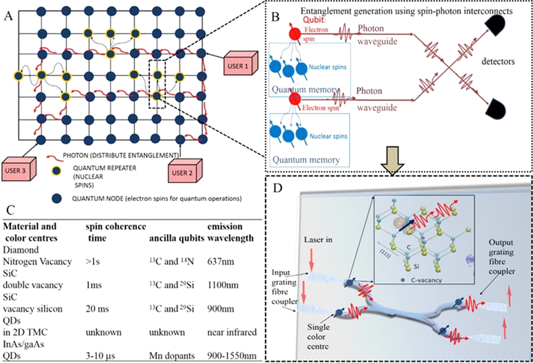
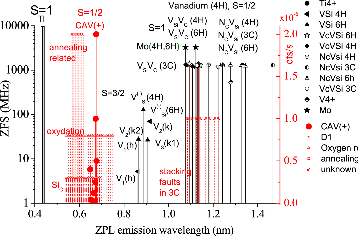
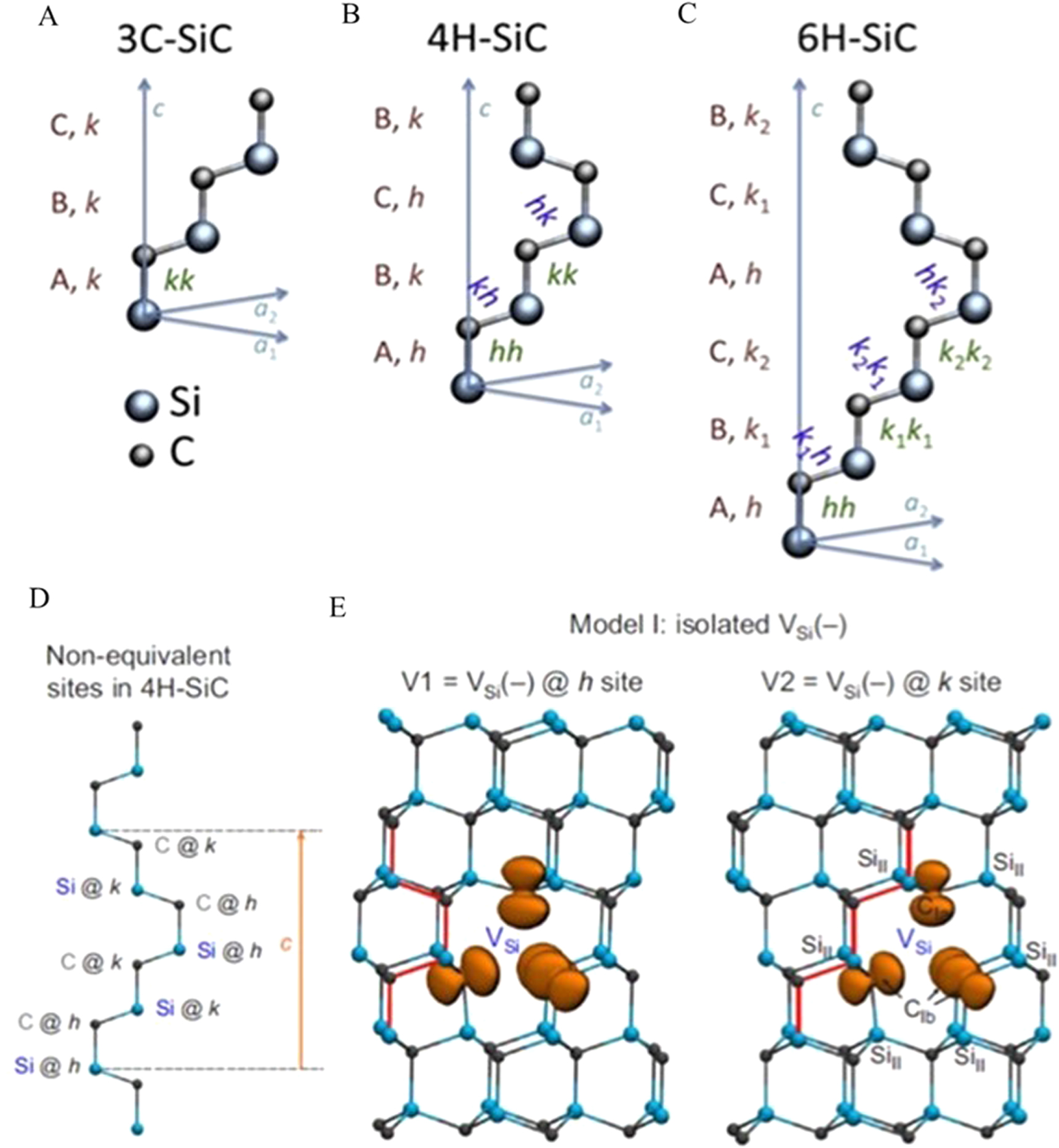
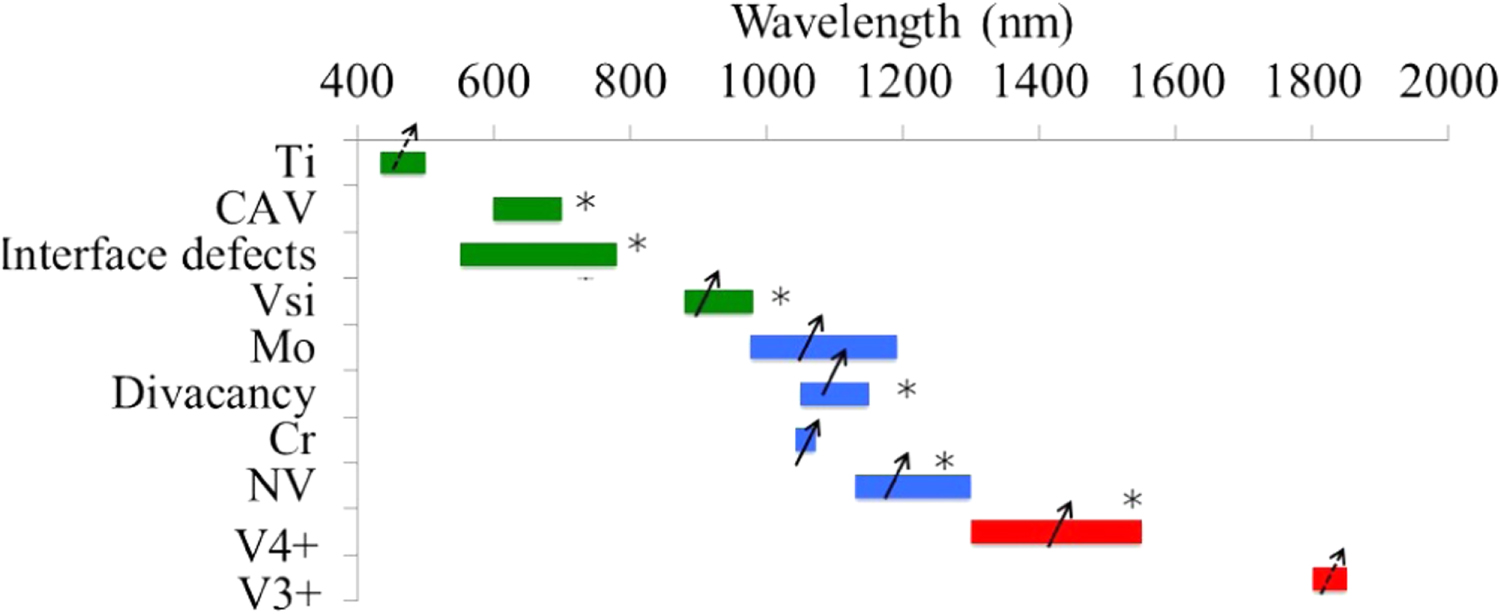
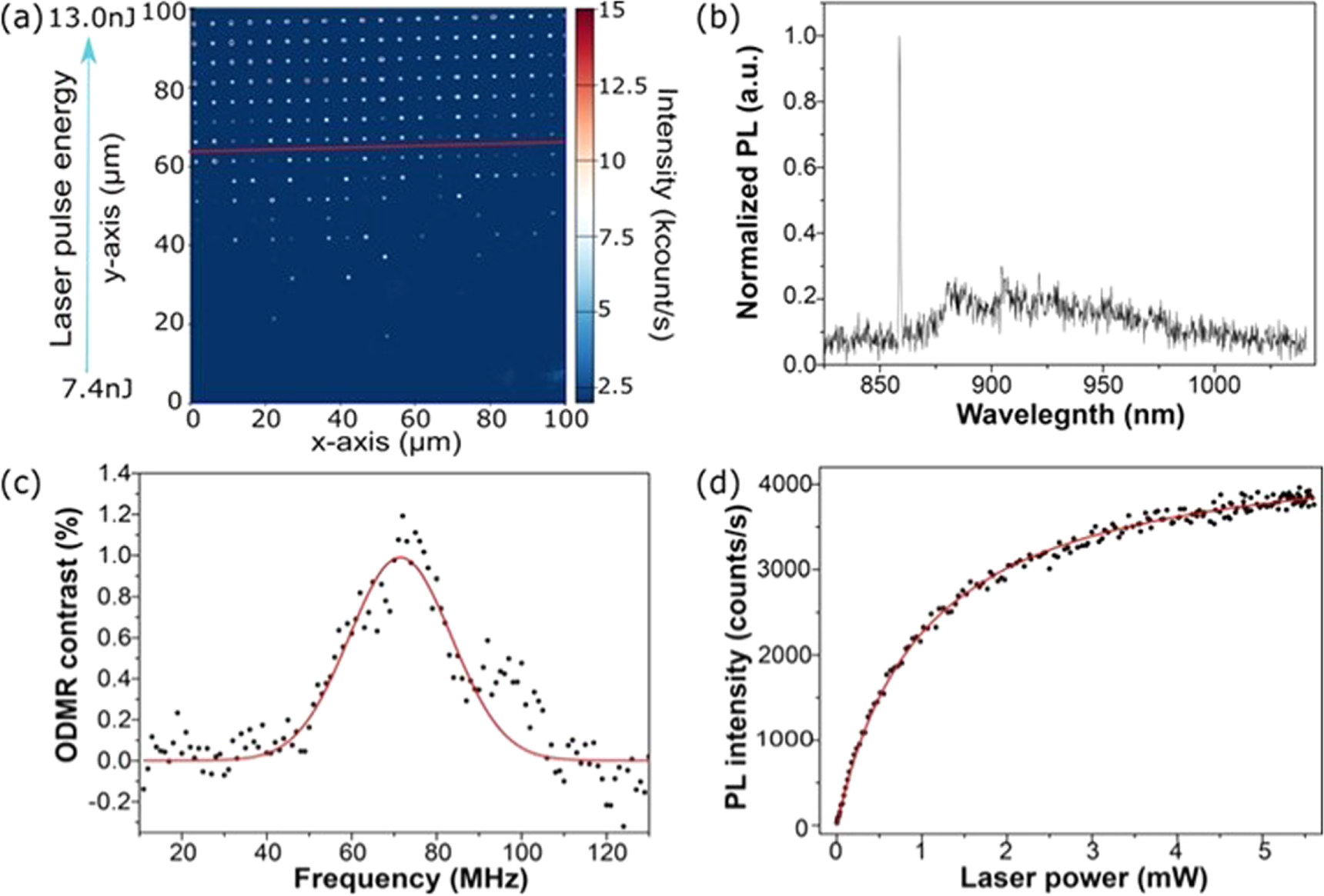
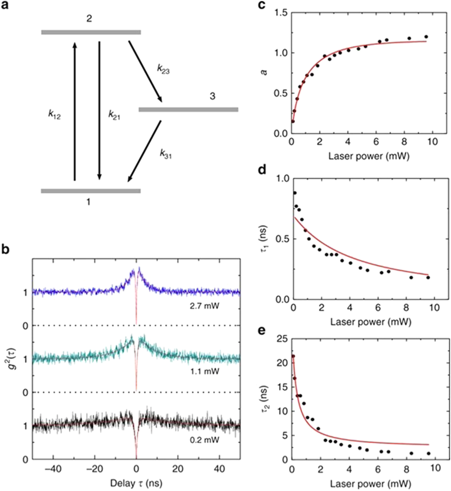
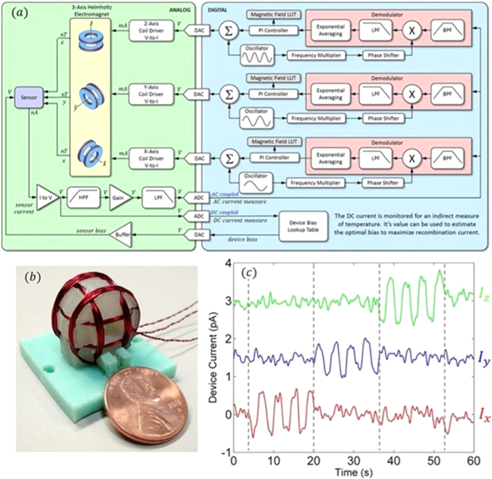
Figure 9. (a) Sketch of the SAW resonator device of [157]. (b) Acoustic focus optical micrograph of the resonator. (c) One-port reflection magnitude (blue) and phase (red) measurements for spin experiments. (d) and (e) Direct s-SXDM measurements using the 4H-SiC [0004] Bragg peak of the mechanical mode from a similar gaussian SAW. Images reprinted by permission from: [Springer Nature Customer Service Centre GmbH]: [Springer Nature] [Nature Physics] [Spin–phonon interactions in silicon carbide addressed by Gaussian acoustics, Whiteley, Wolfowicz, Anderson, Bourassa, Ma, Ye, Koolstra, Satzinger, Holt, Heremans, Cleland, Schuster, Galli and Awschalom), [COPYRIGHT] (2019).
Download figure:
Standard image High-resolution image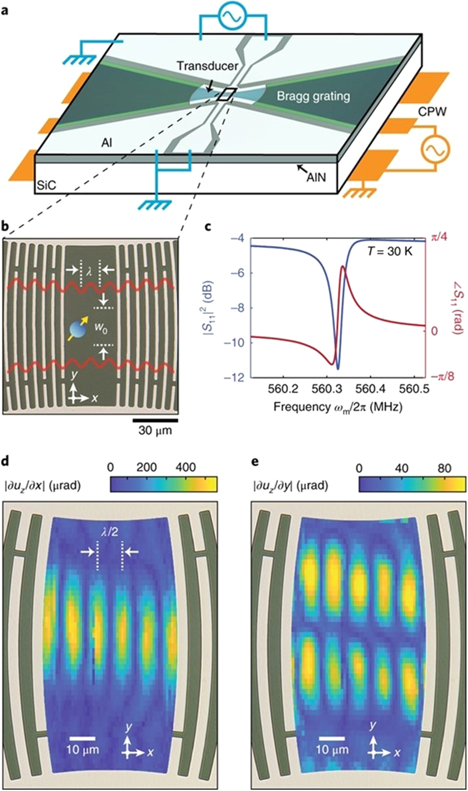
6. Spin-photon entanglement interfaces for quantum metrology and quantum networks
Optically addressable spins in solid-state systems emit photons that can be entangled with their spin. This allows for applications such as quantum communications, metrology and quantum networks. As SiC defects emit at telecommunication wavelength, this makes them excellent candidates for long-range quantum communications. Schemes for spin-photon entanglement in VSi, DV and NV center in SiC defects are proposed [71]. A defect that can support spin-photon entangled interfaces in SiC has been experimentally proved so far as the VSi V2, V1 lines [76], and DV [28, 85]. They possess narrow lifetime-limited optical transitions, according to a theoretical and experimental analysis by photoluminescence excitation (PLE) [70, 78, 80]. Spin-selective resonant optical excitation, in particular, allows reading the spin state of SiC DV and VSi with high fidelity [62, 76]. The high readout fidelity of the spin state is achieved via resonant addressing of different spin transitions between ground and excited state with and without magnetic field. This is possible due to highly symmetric ground and excited state, as the defect's wavefunction symmetry indeed largely decouples its optical transition energy from stray charges in its local environment. Further, limited non-radiative decay transitions, which would introduce spin-flipping or spin-non conservative transitions, can reduce the fidelity of individual defect spin read-out. The emitters' lifetimes in the excited state is around 10 ns [70, 78]. The coupling of such defects with photonic elements such as solid immersion lenses [69], nanowires [159, 160], nanopillars [18] or PhC cavities, microdisks and micro-ring resonators [2, 108, 138, 161–168] enhances/controls the photon flux collection.
Quantum network needs spin-photon entanglement interfaces, where also ancilla qubits are needed. SiC ancilla qubits can be realized by exploiting electron and nuclear spins coupling [169, 170], e.g. in 29Si which shows a hyperfine interaction of up to ∼10 MHz for both VSi and DV, or in 13C. 29Si nuclear spins can show extended excited-state electron-nuclear interaction time which can be exploited to reach near-unity polarization in the DV neutral charge state [171]. Spin-photon interfacing allows for quantum control with near-unity electronic and nuclear polarization, prospecting the use of SiC in photon-mediated entanglement [81].
Quantum metrology relies on quantum theory to describe the physical systems [172] and to provide high-resolution and highly sensitive measurements of their physical parameters, particularly with reference to quantum entanglement [173]. The field promises to develop measurement techniques yielding better precision than the same measurements performed in a classical framework and eventually could supply the most robust metrological standards. At the core of quantum metrology, quantum interference such as Hong–Ou–Mandel interference between indistinguishable single photons is required [9, 174], used also to support long-distance entanglement distribution for quantum network. SiC is currently not yet directly applicable to the field of quantum metrology and as many other systems can be considered as a potential platform. In general quantum entanglement as a resource for quantum metrology remains a theoretical aim. Quantum sensing is a subset of quantum metrology, even if it is often referred to as a distinguished area in quantum technology. In this domain, SiC may have some future further development.
In SiC DV supports the generation of ensemble entangled states of the electron-nuclear-spin, with fidelity as high as 0.9 [64, 175]. As the ZPL width of these emitters is approaching their lifetime (around 80 MHz) in single defects [85], this can permit to achieve single photon indistinguishability for optical quantum interference and entanglement distribution. These achievements are relevant also for quantum networks and quantum cryptography distribution. However, so far, no single-photon source in SiC has been proved experimentally to have single-photon indistinguishability as for other color centers in diamond such as NV and the silicon vacancy. Using the VSi in SiC, it has been demonstrated the manipulation and control of spin qudits (4 dimensions quantum states) [176], owing to the defect 4 projections of their spin states. Higher dimensions quantum states have shown promises to improve quantum metrology [177].
7. Nanophotonics
Nanophotonics in SiC is a high demand as most of the above applications are depending on the successful integration of the above color centers into photonics devices such as photonic crystal cavity, micro-ring resonators, microdisks. While many realizations of optical cavities in SiC have been attempted successfully [36], their optical Q is still far from the predicted values from modeling, indicating that fabrication defects still limit their performance. Further integration of color centers with these cavities [108, 162–164], where moderate Purcell enhancement has been proved, is still quite limited, predominantly due to a lack of reliable methods to fabricate the color center to a specific location. The polytype choice for photonics cavity fabrication has been mostly in 3C with few exceptions where 4H was used. Heteroepitaxial growth of thin layers of cubic 3C-SiC on a Si wafer is a method for building nanophotonic devices [163, 166, 168, 178, 179], and it has been used initially to test the material. However, the quality of the 3C material growth on Si may not allow reaching the required quality factor for implementing quantum photonics as well the defects in 3C SiC are less known than 4H, where most of the above demonstrations have been achieved. The smart-cut techniques applied to hexagonal-polytype thin films grown on oxide [161, 168] have also been used, however, due to the material damage, so far the quality factor achieved is deemed not optimal for the intended applications, where high optical Q is required. Suspended structures can be derived from hexagonal SiC by selective etching, producing devices such as PhC cavities and whispering gallery mode resonators, with quality factors up to 50 000 [11, 164, 165, 180].
Photon collection can be increased tenfold by embedding defects in SiC PhC cavities [108], as Ky5 color center ensembles in 3C-SiC substrates showed optically detected magnetic resonance, assigned to a neutral DV [166]. Microdisk resonators have been built by dopant-selective photoelectrochemical etching of layers fabricated by hexagonal polytype [180], and a nanobeam PhC cavity coupled to a VSi center with a Purcell enhancement of 84 [164, 165], a design that has also been considered with a triangular cross-section [167, 181].
Recently, other approaches have been used to improve the material quality for the fabrication of photonic nanostructures. Both 3C and 4H SiC can be achieved on insulator (SiCOI), based on direct wafer bonding rather than smart cut techniques and thinning of the material, methods now developed at the wafer-scale level. Recent experiments on wafer bonding of 3C on Insulator have provided microdisks with Q = 143 000 [138], while in 4H integrated circuits such as micro-ring resonators [168] with a Q = 73 000, photonic crystal nanocavities [182] with Q = 630 000, and photonics waveguides [183]. Direct wafer bonding holds the promises to improve the final Q and optical quality of the resonators and be able to provide an integrated platform for nonlinear photonics and integrated quantum circuits in SiC.
8. Conclusions and outlook
In this review, we have focused on the latest advances in SiC spin defects control and engineering for quantum applications such as quantum sensing and quantum network. The progress in the field over the past years since its inception has been remarkable. Some of the defects identified as potential qubits, such as DV and VSi, have been further investigated in terms of their suitability as spin-photon interface and both, due to the high fidelity of addressing their spin by using resonance excitation at low temperature, have revealed great potentials for future quantum network application and remote entanglement distribution. Single photons sources in SiC have remarkable properties and are easily integrated with electrical excitation and control within MOSFETs. Additionally, bright emission close to the telecom wavelength at room temperature has been shown even at room temperature. The brightest single-photon sources in SiC do not have optical spin control and their indistinguishability has not yet been proved. It is desirable that in the future some of these emitters could be coupled via dipole–dipole interactions, affecting the coherence time of the spins, with another spin controllable and usable as spin-photon interface defects such as VSi or DV. Conversely, other promising color centers emitting in the IR are still to be understood such as the NV, or Mo in SiC, both holding great promise in this space. It is desirable that more studies should be invested in other color centers to improve the space applicability of this material platform.
One of the challenges remains their fabrication on-demand and with high accuracy, however, 80% yield has been achieved with ions implantation and 30% using direct laser writing. In this direction more studies on increasing the yield of these defects formation and improving their emission collection efficiency should continue, to provide better systems for device engineering for quantum sensing. Based on the ensemble of DV and VSi, some devices have been realized for magnetometry, electrical and strain sensing. Finally, their integration in the nanophotonics cavity remains still limited, regardless of some important recent achievements on methods to improve the quality of SiCOI both in 4H and 3C. However, based on current results on monolithic integration of defects in SiC and improved material performance due to fabrication defects reduction, it is expected a surge of realizations of integrated photonics for qubits in SiC in the next years.